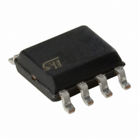
L6385D STMicroelectronics, L6385D Datasheet - Page 4

L6385D
Manufacturer Part Number
L6385D
Description
IC DRIVER HIGH/LOW SIDE 8-SOIC
Manufacturer
STMicroelectronics
Type
Driverr
Datasheet
1.L6385.pdf
(9 pages)
Specifications of L6385D
Configuration
Half Bridge
Input Type
Non-Inverting
Delay Time
110ns
Current - Peak
400mA
Number Of Configurations
1
Number Of Outputs
2
High Side Voltage - Max (bootstrap)
600V
Voltage - Supply
17V
Operating Temperature
-40°C ~ 125°C
Mounting Type
Surface Mount
Package / Case
8-SOIC (3.9mm Width)
Rise Time
50 ns
Fall Time
30 ns
Supply Current
0.32 mA
Maximum Power Dissipation
750 mW
Maximum Operating Temperature
+ 125 C
Mounting Style
SMD/SMT
Minimum Operating Temperature
- 45 C
Number Of Drivers
2
For Use With
497-5492 - EVAL BOARD FOR L6384/L6385/L6386
Lead Free Status / RoHS Status
Lead free / RoHS Compliant
Other names
497-1435-5
497-1435-5
497-3650-5
497-1435-5
497-3650-5
Available stocks
Company
Part Number
Manufacturer
Quantity
Price
Part Number:
L6385D013TR
Manufacturer:
ST
Quantity:
20 000
L6385
Figure 1. Input/Output Timing Diagram
Figure 2. Typical Rise and Fall Times vs.
BOOTSTRAP DRIVER
A bootstrap circuitry is needed to supply the high
voltage section. This function is normally accom-
plished by a high voltage fast recovery diode (fig.
4a). In the L6385 a patented integrated structure
replaces the external diode. It is realized by a
high voltage DMOS, driven synchronously with
the low side driver (LVG), with in series a diode,
as shown in fig. 4b
An internal charge pump (fig. 4b) provides the
DMOS driving voltage .
The diode connected in series to the DMOS has
been added to avoid undesirable turn on of it.
CBOOT selection and charging:
To choose the proper C
MOS can be seen as an equivalent capacitor.
4/9
(nsec)
time
250
200
150
100
50
0
For both high and low side buffers @25˚C Tamb
0
Load Capacitance
1
HVG
LVG
HIN
2
LIN
BOOT
3
value the external
4
Tr
Tf
5
D99IN1054
C (nF)
gate charge :
3nF. With
Figure 3. Quiescent Current vs. Supply
This capacitor C
The ratio between the capacitors C
is proportional to the cyclical voltage loss .
It has to be:
e.g.: if Q
300mV.
If HVG has to be supplied for a long time, the
C
( A)
10
10
10
10
Iq
BOOT
4
3
2
0
selection has to take into account also the
2
gate
Voltage
C
BOOT
4
is 30nC and V
C
EXT
BOOT
C
6
D99IN1053
= 100nF the drop would be
EXT
is related to the MOS total
>>>C
8
Q
V
10
gate
gate
EXT
gate
12
is 10V, C
EXT
14
and C
D99IN1055
16 V
EXT
BOOT
S
(V)
is


