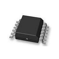
VN5050J-E STMicroelectronics, VN5050J-E Datasheet - Page 10

VN5050J-E
Manufacturer Part Number
VN5050J-E
Description
IC DRVR HIGHSIDE AUTO PWRSSO-12
Manufacturer
STMicroelectronics
Type
High Sider
Datasheet
1.VN5050JTR-E.pdf
(31 pages)
Specifications of VN5050J-E
Input Type
Non-Inverting
Number Of Outputs
1
On-state Resistance
50 mOhm
Current - Peak Output
19A
Voltage - Supply
4.5 V ~ 36 V
Operating Temperature
-40°C ~ 150°C
Mounting Type
Surface Mount
Package / Case
PowerSSO-12
Product
Driver ICs - Various
Supply Voltage (max)
36 V
Supply Voltage (min)
4.5 V
Supply Current
0.005 mA
Maximum Operating Temperature
+ 150 C
Mounting Style
SMD/SMT
Maximum Turn-off Delay Time
35000 ns
Maximum Turn-on Delay Time
20000 ns
Minimum Operating Temperature
- 40 C
Number Of Drivers
1
Device Type
High Side
Module Configuration
High Side
Peak Output Current
19A
Output Resistance
0.065ohm
Input Delay
20µs
Output Delay
35µs
Supply Voltage Range
4.5V To 36V
Rohs Compliant
Yes
Lead Free Status / RoHS Status
Lead free / RoHS Compliant
Current - Output / Channel
-
Lead Free Status / Rohs Status
Lead free / RoHS Compliant
Available stocks
Company
Part Number
Manufacturer
Quantity
Price
Part Number:
VN5050J-E
Manufacturer:
ST
Quantity:
20 000
Electrical specifications
10/31
Table 8.
Table 9.
(1) To ensure long term reliability under heavy overload or short circuit conditions, protection and related
Symbol
Symbol
V
I
C
V
V
LSTAT
T
diagnostic signals must be used together with a proper software strategy. If the device is subjected to
abnormal conditions, this software must limit the duration and number of activation cycles.
T
DEMAG
STAT
I
STAT
I
t
V
T
SCL
HYST
limH
SDL
limL
T
TSD
RS
ON
R
Status low output
voltage
Status leakage current
Status pin input
capacitance
Status clamp voltage
DC short circuit current
Short circuit current
during thermal cycling
Shutdown temperature
Reset temperature
Thermal reset of
STATUS
Thermal hysteresis
(T
Status delay in overload
conditions
Turn-Off output voltage
clamp
Output voltage drop
limitation
Status pin (V
Protections
TSD
Parameter
-T
Parameter
R
)
(1)
SD
=0V)
I
Normal Operation or V
V
Normal Operation or V
V
I
I
STAT
STAT
STAT
STAT
STAT
V
5V<V
V
T
T
I
I
T
(see
OUT
OUT
= 1.6 mA, V
= 1mA
= -1mA
R
j
j
CC
CC
= 5V
= 5V
>T
= -40°C...+150°C
<T
= 13V
= 13V
Test conditions
TSD
=2A; V
= 0.1A;
Figure
j
CC
<T
Test conditions
<36V
TSD
(see
IN
6)
SD
=0; L=6mH
Figure
=0V
SD
SD
4)
=5V,
=5V,
T
V
Min.
13.5
RS
150
135
CC
Min.
5.5
-41 V
+ 1 T
Typ.
RS
CC
175
Typ.
-0.7
19
25
7
7
-46 V
+ 5
Max.
Max.
26.5
26.5
200
CC
100
0.5
20
VN5050J-E
10
7
-52
Unit
Unit
mV
µA
pF
°C
°C
°C
°C
µs
A
A
A
V
V
V
V


