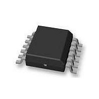
VN5050J-E STMicroelectronics, VN5050J-E Datasheet - Page 6

VN5050J-E
Manufacturer Part Number
VN5050J-E
Description
IC DRVR HIGHSIDE AUTO PWRSSO-12
Manufacturer
STMicroelectronics
Type
High Sider
Datasheet
1.VN5050JTR-E.pdf
(31 pages)
Specifications of VN5050J-E
Input Type
Non-Inverting
Number Of Outputs
1
On-state Resistance
50 mOhm
Current - Peak Output
19A
Voltage - Supply
4.5 V ~ 36 V
Operating Temperature
-40°C ~ 150°C
Mounting Type
Surface Mount
Package / Case
PowerSSO-12
Product
Driver ICs - Various
Supply Voltage (max)
36 V
Supply Voltage (min)
4.5 V
Supply Current
0.005 mA
Maximum Operating Temperature
+ 150 C
Mounting Style
SMD/SMT
Maximum Turn-off Delay Time
35000 ns
Maximum Turn-on Delay Time
20000 ns
Minimum Operating Temperature
- 40 C
Number Of Drivers
1
Device Type
High Side
Module Configuration
High Side
Peak Output Current
19A
Output Resistance
0.065ohm
Input Delay
20µs
Output Delay
35µs
Supply Voltage Range
4.5V To 36V
Rohs Compliant
Yes
Lead Free Status / RoHS Status
Lead free / RoHS Compliant
Current - Output / Channel
-
Lead Free Status / Rohs Status
Lead free / RoHS Compliant
Available stocks
Company
Part Number
Manufacturer
Quantity
Price
Part Number:
VN5050J-E
Manufacturer:
ST
Quantity:
20 000
Block diagram and pin description
Note:
6/31
Figure 2.
The above pin configuration reflects the changes notified with PCN-APG-BOD/07/2886. The
new pinout is backaward compatible with existing PCB layouts where pins #1 and #6 are
connected to Vcc and/or pins #7 and 12 are connected to OUTPUT. For new PCB designs,
these pins should be left unconnected.
Table 3.
(1) Not recommended.
Floating
To ground
Connection / Pin
Configuration diagram (top view)
Suggested connections for unused and N.C. pins
STATUS_DIS
STATUS
INPUT
STATUS
GND
N.R.
N.C.
N.C.
X
(1)
PowerSSO-12
1
2
3
4
5
6
N.C.
X
X
OUTPUT
12
11
10
N.R.
9
8
7
X
TAB = V
N.C.
OUTPUT
OUTPUT
OUTPUT
OUTPUT
N.C.
Through 10KΩ
resistor
INPUT
cc
X
Through 10KΩ
STAT_DIS
VN5050J-E
resistor
X


