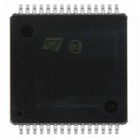
VNH3ASP30-E STMicroelectronics, VNH3ASP30-E Datasheet - Page 21

VNH3ASP30-E
Manufacturer Part Number
VNH3ASP30-E
Description
IC MOTOR DVR H BRDG 30-MPSO
Manufacturer
STMicroelectronics
Type
Half Bridge DC Motor Driverr
Datasheet
1.VNH3ASP30TR-E.pdf
(33 pages)
Specifications of VNH3ASP30-E
Applications
Automotive
Number Of Outputs
2
Current - Output
30A
Voltage - Supply
5.5 V ~ 16 V
Operating Temperature
-40°C ~ 150°C
Mounting Type
Surface Mount
Package / Case
30-MPSO, MultiPowerSO
Supply Current
10 mA
Mounting Style
SMD/SMT
Device Type
Motor
Module Configuration
Full Bridge
Peak Output Current
30A
Output Resistance
0.03ohm
Input Delay
250µs
Output Delay
250µs
Supply Voltage Range
5.5V To 36V
Rohs Compliant
Yes
Lead Free Status / RoHS Status
Lead free / RoHS Compliant
Voltage - Load
-
Lead Free Status / Rohs Status
Lead free / RoHS Compliant
Available stocks
Company
Part Number
Manufacturer
Quantity
Price
Part Number:
VNH3ASP30-E
Manufacturer:
ST
Quantity:
20 000
VNH3ASP30-E
3.1
Note:
When a fault condition is detected, the user can know which power element is in fault by
monitoring the IN
In any case, when a fault is detected, the faulty leg of the bridge is latched off. To turn on the
respective output (OUT
Reverse battery protection
Three possible solutions can be considered:
a Schottky diode D connected to V
an N-channel MOSFET connected to the GND pin (see
for DC to 20 kHz PWM operation short circuit protection on page
a P-channel MOSFET connected to the V
The device sustains no more than -30A in reverse battery conditions because of the two
body diodes of the power MOSFETs. Additionally, in reverse battery condition the I/Os of
are pulled down to the V
limit the current sunk from the microcontroller I/Os. If I
current through µC I/Os, the series resistor is:
Figure 33. Half-bridge configuration
The VNH3ASP30-E can be used as a high power half-bridge driver achieving an On
resistance per leg of 21 mΩ .
OUT
IN
IN
DIAG
PWM
DIAG
A
B
A
A
B
GND
/EN
/EN
B
A
A
A
, IN
GND
B
, DIAG
X
CC
) again, the input signal must rise from low to high level.
B
OUT
line (approximately -1.5V). A series resistor must be inserted to
B
A
/EN
CC
A
and DIAG
R
pin
V
=
CC
CC
V
-------------------------------- -
IOs
M
I Rmax
pin
B
–
/EN
V
CC
B
pins.
Rmax
Figure 32: Typical application circuit
is the maximum target reverse
OUT
A
20)
GND
Application information
A
GND
DIAG
DIAG
B
A
B
PWM
OUT
/EN
/EN
IN
IN
A
B
B
A
B
21/33


