LP3971SQ-2G16/NOPB National Semiconductor, LP3971SQ-2G16/NOPB Datasheet - Page 7
LP3971SQ-2G16/NOPB
Manufacturer Part Number
LP3971SQ-2G16/NOPB
Description
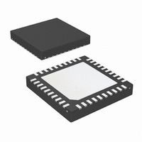
IC PMU FOR APPL PROCESSORS 40LLP
Manufacturer
National Semiconductor
Series
PowerWise®r
Datasheet
1.LP3971SQ-B510NOPB.pdf
(50 pages)
Specifications of LP3971SQ-2G16/NOPB
Applications
Processor
Current - Supply
60µA
Voltage - Supply
2.7 V ~ 5.5 V
Operating Temperature
-40°C ~ 85°C
Mounting Type
Surface Mount
Package / Case
40-LLP
Lead Free Status / RoHS Status
Lead free / RoHS Compliant
Other names
LP3971SQ-2G16
LP3971SQ-2G16
LP3971SQ-2G16TR
LP3971SQ-2G16
LP3971SQ-2G16TR


Pin Descriptions
Pin #
10
11
12
13
14
15
16
17
18
19
20
21
22
23
24
25
26
27
28
29
30
31
32
33
1
2
3
4
5
6
7
8
9
V
EXT_WAKEUP
OUT
V
nBATT_FLT
nTEST_JIG
V
V
V
V
V
nCHG_EN
V
V
PWR_ON
V
IN
V
OUT
OUT
OUT
OUT
OUT
GPIO1 /
SPARE
PGND2
nRSTO
PGND3
IN
GPIO2
IN
IN
IN
nRSTI
GND1
VDDA
Name
VREF
BUBATT
LDO_RTC
SW2
SW3
SDA
SCL
FB1
FB2
FB3
V
Buck2
Buck3
LDO4
LDO5
IN
LDO1
LDO2
LDO3
LDO4
LDO5
I/O
I/O
I/O
I/O
O
O
O
G
O
O
O
O
O
G
O
O
O
O
G
I
I
I
I
I
I
I
I
I
I
I
I
I
I
I
Type
PWR
PWR
PWR
PWR
PWR
PWR
PWR
PWR
PWR
PWR
PWR
PWR
PWR
PWR
PWR
D
D
D
D
A
D
G
A
D
G
D
D
A
D
A
D
D
G
This is an active HI push button input which can be used to signal PWR_ON
and PWR_OFF events to the CPU by controlling the ext_wakup [pin4] and
select contents of register 8H'02
This is an active LOW input signal used for detecting an external HW event.
The response is seen in the ext_wakup [pin4] and select contents of register
8H'02
This is an input signal used for detecting a external HW event. The response
is seen in the ext_wakup [pin4] and select contents of register 8H'02. The
polarity on this pin is assignable
This pin generates a single 10mS pulse output to CPU in response to input
from pin[s] 1, 2, and 3. Flags CPU to interrogate register 8H'02
Buck1 input feedback terminal
Battery Input (Internal circuitry and LDO1-3 power input)
LDO1 output
LDO2 output
Active low Reset pin. Signal used to reset the IC (by default is pulled high
internally). Typically a push button reset.
Ground
Bypass Cap. for the high internal impedance reference.
LDO3 output
LDO4 output
Power input to LDO4, this can be connected to either from a 1.8V supply to
main Battery supply.
Back Up Battery input supply.
LDO_RTC output supply to the RTC of the application processor.
Main Battery fault output, indicates the main battery is low
(discharged) or the dc source has been removed from the system. This gives
the processor an indicator that the power will shut down. During this time the
processor will operate from the back up coin cell.
Buck2 NMOS Power Ground
Buck2 switcher output
Battery input power to Buck2
I
I
Buck2 input feedback terminal
Reset output from the PMIC to the processor
LDO5 output
Power input to LDO5, this can be connected to V
supply.
Analog Power for VREF, BIAS
Buck3 Feedback
General Purpose I/O / Ext. backup battery charger enable pin. This pin
enables the main battery / DC source power to charge the backup battery.
This pin toggled via the application processor. By grounding this pin the DC
source continuously charges the backup battery
General Purpose I/O
Battery input power to Buck3
Buck3 switcher output
Buck3 NMOS Power Ground
2
2
C Data (Bidirectional)
C Clock
7
Description
IN
or to a separate 1.8V
www.national.com
Related parts for LP3971SQ-2G16/NOPB
Image
Part Number
Description
Manufacturer
Datasheet
Request
R

Part Number:
Description:
IC,Multiple Regulator Circuit,CMOS,LLCC,40PIN,PLASTIC
Manufacturer:
National Semiconductor

Part Number:
Description:
IC PMU FOR APPL PROCESSORS 40LLP
Manufacturer:
National Semiconductor
Datasheet:
Part Number:
Description:
IC PMU FOR APPL PROCESSORS 40LLP
Manufacturer:
National Semiconductor
Datasheet:
Part Number:
Description:
IC PMU FOR APPL PROCESSORS 40LLP
Manufacturer:
National Semiconductor
Datasheet:
Part Number:
Description:
IC PMU FOR ADV APPLICATION 40LLP
Manufacturer:
National Semiconductor
Datasheet:
Part Number:
Description:
IC PMU FOR APPL PROCESSOR 40-LLP
Manufacturer:
National Semiconductor
Datasheet:
Part Number:
Description:
IC PMU FOR ADV APPL PROC 40-LLP
Manufacturer:
National Semiconductor
Datasheet:
Part Number:
Description:
IC PMU MULTI FUNCT PROGR 40-LLP
Manufacturer:
National Semiconductor
Datasheet:
Part Number:
Description:
IC PMU FOR APPL PROCESSOR 40-LLP
Manufacturer:
National Semiconductor
Datasheet:
Part Number:
Description:
IC PMU FOR APPL PROCESSOR 40-LLP
Manufacturer:
National Semiconductor
Datasheet:
Part Number:
Description:
IC PMU FOR ADV APPLICATION 40LLP
Manufacturer:
National Semiconductor
Datasheet:
Part Number:
Description:
IC PMU FOR ADV APPLICATION 40LLP
Manufacturer:
National Semiconductor
Datasheet:
Part Number:
Description:
IC PMU MULTI FUNCT PROGR 40-LLP
Manufacturer:
National Semiconductor
Datasheet:
Part Number:
Description:
IC PMU FOR APPL PROCESSORS 40LLP
Manufacturer:
National Semiconductor
Datasheet:
Part Number:
Description:
IC,Multiple Regulator Circuit,CMOS,LLCC,40PIN,PLASTIC
Manufacturer:
National Semiconductor