LM2702MT-ADJ/NOPB National Semiconductor, LM2702MT-ADJ/NOPB Datasheet - Page 17
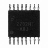
LM2702MT-ADJ/NOPB
Manufacturer Part Number
LM2702MT-ADJ/NOPB
Description
IC MODULE PANEL TFT DISP 16TSSOP
Manufacturer
National Semiconductor
Datasheet
1.LM2702MT-ADJNOPB.pdf
(21 pages)
Specifications of LM2702MT-ADJ/NOPB
Applications
LCD Display
Current - Supply
2.6mA
Voltage - Supply
2.2 V ~ 12 V
Operating Temperature
-40°C ~ 125°C
Mounting Type
Surface Mount
Package / Case
16-TSSOP
Lead Free Status / RoHS Status
Lead free / RoHS Compliant
Other names
*LM2702MT-ADJ
*LM2702MT-ADJ/NOPB
LM2702MT-ADJ
*LM2702MT-ADJ/NOPB
LM2702MT-ADJ


Operation
where R
approximately 1MΩ. For most applications, performance can
be optimized by choosing values within the range 5kΩ ≤ R
≤ 40kΩ (R
Output Capacitor ESR Compensation) and 680pF ≤ C
4.7nF. Refer to the Typical Application Circuit and the Appli-
cations Information section for recommended values for spe-
cific circuits and conditions. Refer to the Compensation sec-
tion for other design requirement.
COMPENSATION FOR BOOST DC/DC
This section will present a general design procedure to help
insure a stable and operational circuit. The designs in this
datasheet are optimized for particular requirements. If differ-
ent conversions are required, some of the components may
need to be changed to ensure stability. Below is a set of
general guidelines in designing a stable circuit for continu-
ous conduction operation (Inductor current never reaches
zero), in most all cases this will provide for stability during
discontinuous operation as well. The power components and
their effects will be determined first, then the compensation
components will be chosen to produce stability.
INDUCTOR AND DIODE SELECTION
Although the inductor size mentioned earlier is fine for most
applications, a more exact value can be calculated. To en-
sure stability at duty cycles above 50%, the inductor must
have some minimum value determined by the minimum
input voltage and the maximum output voltage. This equa-
tion is:
where fs is the switching frequency, D is the duty cycle, and
R
the graph "R
acteristics section. This equation is only good for duty cycles
greater than 50% (D
recommended values may be used. The corresponding in-
ductor current ripple as shown in Figure 2 (a) is given by:
The inductor ripple current is important for a few reasons.
One reason is because the peak switch current will be the
average inductor current (input current or I
As a side note, discontinuous operation occurs when the
inductor current falls to zero during a switching cycle, or ∆i
is greater than the average inductor current. Therefore, con-
tinuous conduction mode occurs when ∆i
average inductor current. Care must be taken to make sure
that the switch will not reach its current limit during normal
operation. The inductor must also be sized accordingly. It
should have a saturation current rating higher than the peak
inductor current expected. The output and input voltage
ripples are also affected by the total ripple current.
DSON
is the ON resistance of the internal switch taken from
O
C
is the output impedance of the error amplifier,
DSON
can be up to 200kΩ if C
vs. V
(Continued)
>
0.5), for duty cycles less than 50% the
IN
" in the Typical Performance Char-
C2
is used, see High
L
LOAD
is less than the
/D’) plus ∆i
C
L
C
≤
L
.
17
The output diode for a boost regulator must be chosen
correctly depending on the output voltage and the output
current. The typical current waveform for the diode in con-
tinuous conduction mode is shown in Figure 2 (b). The diode
must be rated for a reverse voltage equal to or greater than
the output voltage used. The average current rating must be
greater than the maximum load current expected, and the
peak current rating must be greater than the peak inductor
current. During short circuit testing, or if short circuit condi-
tions are possible in the application, the diode current rating
must exceed the switch current limit. Using Schottky diodes
with lower forward voltage drop will decrease power dissipa-
tion and increase efficiency.
DC GAIN AND OPEN-LOOP GAIN
Since the control stage of the converter forms a complete
feedback loop with the power components, it forms a closed-
loop system that must be stabilized to avoid positive feed-
back and instability. A value for open-loop DC gain will be
required, from which you can calculate, or place, poles and
zeros to determine the crossover frequency and the phase
margin. A high phase margin (greater than 45˚) is desired for
the best stability and transient response. For the purpose of
stabilizing the LM2702, choosing a crossover point well be-
low where the right half plane zero is located will ensure
sufficient phase margin. A discussion of the right half plane
zero and checking the crossover using the DC gain will
follow.
INPUT AND OUTPUT CAPACITOR SELECTION
The switching action of a boost regulator causes a triangular
voltage waveform at the input. A capacitor is required to
reduce the input ripple and noise for proper operation of the
regulator. The size used depends on the application and
board layout. If the regulator will be loaded uniformly, with
very little load changes, and at lower current outputs, the
input capacitor size can often be reduced. The size can also
be reduced if the input of the regulator is very close to the
source output. The size will generally need to be larger for
applications where the regulator is supplying nearly the
maximum rated output or if large load steps are expected. A
minimum value of 10µF should be used for the less stressful
conditions while a 22µF to 47µF capacitor may be required
for higher power and dynamic loads. Larger values and/or
lower ESR may be needed if the application requires very
low ripple on the input source voltage.
The choice of output capacitors is also somewhat arbitrary
and depends on the design requirements for output voltage
ripple. It is recommended that low ESR (Equivalent Series
Resistance, denoted R
ceramic, polymer electrolytic, or low ESR tantalum. Higher
ESR capacitors may be used but will require more compen-
sation which will be explained later on in the section. The
ESR is also important because it determines the peak to
peak output voltage ripple according to the approximate
equation:
A minimum value of 10µF is recommended and may be
increased to a larger value. After choosing the output capaci-
tor you can determine a pole-zero pair introduced into the
control loop by the following equations:
∆V
OUT
) 2∆i
ESR
) capacitors be used such as
L
R
ESR
(in Volts)
www.national.com
Related parts for LM2702MT-ADJ/NOPB
Image
Part Number
Description
Manufacturer
Datasheet
Request
R

Part Number:
Description:
Tft Panel Module
Manufacturer:
National Semiconductor Corporation
Datasheet:

Part Number:
Description:
National Semiconductor [8-Bit D/A Converter]
Manufacturer:
National Semiconductor
Datasheet:
Part Number:
Description:
National Semiconductor [Media Coprocessor]
Manufacturer:
National Semiconductor
Datasheet:
Part Number:
Description:
Digitally Controlled Tone and Volume Circuit with Stereo Audio Power Amplifier, Microphone Preamp Stage and National 3D Sound
Manufacturer:
National Semiconductor
Datasheet:
Part Number:
Description:
Digitally Controlled Tone and Volume Circuit with Stereo Audio Power Amplifier, Microphone Preamp Stage and National 3D Sound
Manufacturer:
National Semiconductor
Datasheet:
Part Number:
Description:
AC97 Rev 2 Codec with Sample Rate Conversion and National 3D Sound
Manufacturer:
National Semiconductor
Part Number:
Description:
Manufacturer:
National Semiconductor
Datasheet:
Part Number:
Description:
Manufacturer:
National Semiconductor
Datasheet:
Part Number:
Description:
General Purpose, Low Voltage, Low Power, Rail-to-Rail Output Operational Amplifiers
Manufacturer:
National Semiconductor
Datasheet:
Part Number:
Description:
8-bit 20 MSPS flash A/D converter.
Manufacturer:
National Semiconductor
Datasheet:
Part Number:
Description:
Low Noise Quad Operational Amplifier
Manufacturer:
National Semiconductor
Datasheet:
Part Number:
Description:
Quad Differential Line Receivers
Manufacturer:
National Semiconductor
Datasheet:
Part Number:
Description:
Quad High Speed Trapezoidal? Bus Transceiver
Manufacturer:
National Semiconductor
Datasheet:
Part Number:
Description:
Dual Line Receiver
Manufacturer:
National Semiconductor
Datasheet: