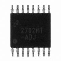
LM2702MT-ADJ/NOPB National Semiconductor, LM2702MT-ADJ/NOPB Datasheet - Page 18

LM2702MT-ADJ/NOPB
Manufacturer Part Number
LM2702MT-ADJ/NOPB
Description
IC MODULE PANEL TFT DISP 16TSSOP
Manufacturer
National Semiconductor
Datasheet
1.LM2702MT-ADJNOPB.pdf
(21 pages)
Specifications of LM2702MT-ADJ/NOPB
Applications
LCD Display
Current - Supply
2.6mA
Voltage - Supply
2.2 V ~ 12 V
Operating Temperature
-40°C ~ 125°C
Mounting Type
Surface Mount
Package / Case
16-TSSOP
Lead Free Status / RoHS Status
Lead free / RoHS Compliant
Other names
*LM2702MT-ADJ
*LM2702MT-ADJ/NOPB
LM2702MT-ADJ
*LM2702MT-ADJ/NOPB
LM2702MT-ADJ
www.national.com
Operation
Where R
the maximum load current. The zero created by the ESR of
the output capacitor is generally very high frequency if the
ESR is small. If low ESR capacitors are used it can be
neglected. If higher ESR capacitors are used see the High
Output Capacitor ESR Compensation section.
RIGHT HALF PLANE ZERO
A current mode control boost regulator has an inherent right
half plane zero (RHP zero). This zero has the effect of a zero
in the gain plot, causing an imposed +20dB/decade on the
rolloff, but has the effect of a pole in the phase, subtracting
another 90˚ in the phase plot. This can cause undesirable
effects if the control loop is influenced by this zero. To ensure
the RHP zero does not cause instability issues, the control
loop should be designed to have a bandwidth of less than
the frequency of the RHP zero. This zero occurs at a fre-
quency of:
where I
SELECTING THE COMPENSATION COMPONENTS
The first step in selecting the compensation components R
and C
loop. Simply choose values for R
given in the Introduction to Compensation section to set this
pole in the area of 10Hz to 500Hz. The frequency of the pole
created is determined by the equation:
where R
approximately 1MΩ. Since R
R
can be neglected until a value is chosen to set the zero f
f
capacitor, f
ent load currents as shown by the equation, so setting the
zero is not exact. Determine the range of f
pected loads and then set the zero f
mately in the middle. The frequency of this zero is deter-
mined by:
Now R
Check to make sure that the pole f
500Hz range, change each value slightly if needed to ensure
both component values are in the recommended range. After
checking the design at the end of this section, these values
can be changed a little more to optimize performance if
desired. This is best done in the lab on a bench, checking the
load step response with different values until the ringing and
overshoot on the output voltage at the edge of the load steps
is minimal. This should produce a stable, high performance
ZC
O
, it does not have much effect on the above equation and
is created to cancel out the pole created by the output
C
C
LOAD
is to set a dominant low frequency pole in the control
O
L
can be chosen with the selected value for C
is the minimum load resistance corresponding to
P1
is the output impedance of the error amplifier,
is the maximum load current.
. The output capacitor pole will shift with differ-
(Continued)
C
is generally much less than
C
and C
PC
ZC
is still in the 10Hz to
C
to a point approxi-
within the ranges
P1
over the ex-
ZC
1
C
⁄
C
2
.
.
18
circuit. For improved transient response, higher values of R
should be chosen. This will improve the overall bandwidth
which makes the regulator respond more quickly to tran-
sients. If more detail is required, or the most optimal perfor-
mance is desired, refer to a more in depth discussion of
compensating current mode DC/DC switching regulators.
HIGH OUTPUT CAPACITOR ESR COMPENSATION
When using an output capacitor with a high ESR value, or
just to improve the overall phase margin of the control loop,
another pole may be introduced to cancel the zero created
by the ESR. This is accomplished by adding another capaci-
tor, C
parallel with the series combination of R
should be placed at the same frequency as f
zero. The equation for this pole follows:
To ensure this equation is valid, and that C
without negatively impacting the effects of R
must be greater than 10f
CHECKING THE DESIGN
The final step is to check the design. This is to ensure a
bandwidth of
This is done by calculating the open-loop DC gain, A
this value is known, you can calculate the crossover visually
by placing a −20dB/decade slope at each pole, and a +20dB/
decade slope for each zero. The point at which the gain plot
crosses unity gain, or 0dB, is the crossover frequency. If the
crossover frequency is less than
margin should be high enough for stability. The phase mar-
gin can also be improved by adding C
in the section. The equation for A
additional equations required for the calculation:
where R
mum input voltage, g
tance found in the Electrical Characteristics table, and R
SON
the Typical Performance Characteristics section.
is the value chosen from the graph "R
C2
, directly from the compensation pin V
L
is the minimum load resistance, V
1
⁄
2
or less of the frequency of the RHP zero.
mc ) 0.181fs (in V/s)
m
is the error amplifier transconduc-
ZC
.
1
⁄
2
the RHP zero, the phase
DC
C2
is given below with
as discussed earlier
C
and C
DSON
C2
C
C
IN
and C
can be used
to ground, in
Z1
is the mini-
C
vs. V
, the ESR
. The pole
DC
C
. After
IN
, f
PC2
" in
D -
C


