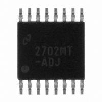
LM2702MT-ADJ/NOPB National Semiconductor, LM2702MT-ADJ/NOPB Datasheet - Page 7

LM2702MT-ADJ/NOPB
Manufacturer Part Number
LM2702MT-ADJ/NOPB
Description
IC MODULE PANEL TFT DISP 16TSSOP
Manufacturer
National Semiconductor
Datasheet
1.LM2702MT-ADJNOPB.pdf
(21 pages)
Specifications of LM2702MT-ADJ/NOPB
Applications
LCD Display
Current - Supply
2.6mA
Voltage - Supply
2.2 V ~ 12 V
Operating Temperature
-40°C ~ 125°C
Mounting Type
Surface Mount
Package / Case
16-TSSOP
Lead Free Status / RoHS Status
Lead free / RoHS Compliant
Other names
*LM2702MT-ADJ
*LM2702MT-ADJ/NOPB
LM2702MT-ADJ
*LM2702MT-ADJ/NOPB
LM2702MT-ADJ
Gamma Buffer
AV
Is+
I
PMOS Switch Logic Control
I
R
I
I
V
SC
DELAY
SWO
SWI
SWC
DSON
Electrical Characteristics Gamma Buffer
Specifications in standard type face are for T
ture Range ( T
C
Electrical Characteristics PMOS Switch Logic Control
Specifications in standard type face are for T
ture Range ( T
C
Note 1: The maximum allowable power dissipation is a function of the maximum junction temperature, T
and the ambient temperature, T
at any ambient temperature is calculated using: P
temperature, and the regulator will go into thermal shutdown.
Note 2: Absolute maximum ratings are limits beyond which damage to the device may occur. Operating Ratings are conditions for which the device is intended to
be functional, but device parameter specifications may not be guaranteed. For guaranteed specifications and test conditions, see the Electrical Characteristics.
Note 3: The human body model is a 100 pF capacitor discharged through a 1.5kΩ resistor into each pin. The machine model is a 200pF capacitor discharged
directly into each pin.
Note 4: Vcom pin is rated for 1.5kV Human Body Model and 150V Machine Model.
Note 5: All limits guaranteed at room temperature (standard typeface) and at temperature extremes (bold typeface). All room temperature limits are 100%
production tested or guaranteed through statistical analysis. All limits at temperature extremes are guaranteed via correlation using standard Statistical Quality
Control (SQC) methods. All limits are used to calculate Average Outgoing Quality Level (AOQL).
Note 6: Typical numbers are at 25˚C and represent the most likely norm.
Note 7: Duty cycle affects current limit due to ramp generator. Current limit is at 0% duty cycle and will decrease with higher duty cycles. See Typical Performance
Characteristics for a graph of Power Switch Current Limit vs. V
Note 8: See the graph titled "R
Note 9: Bias current flows into FB pin.
Note 10: Refer to the graphs titled "Input Offset Voltage vs. Common Mode Voltage".
Symbol
Symbol
IN
GAMMA
GAMMA
= 1nF.
= 1nF.
Supply Voltage
Supply Current (Amplifier +
Buffer)
Output Short Circuit Current
Delay Current
PMOS Switch ON Resistance
PMOS Switch Current
PMOS Switch Input Current
Switch ON
Switch OFF
J
J
= −40˚C to +125˚C). Unless otherwise specified, V
= −40˚C to +125˚C). Unless otherwise specified, V
Parameter
Parameter
A
DSON
. See the Electrical Characteristics table for the thermal resistance of various layouts. The maximum allowable power dissipation
vs. V
IN
" for a more accurate value of the power switch R
D
(MAX) = (T
Vo = AV
Source
Sink
Switch ON
SWC = 0V, SWO Open, SWI
= 30V
SWC = 1.7V, SWO Open,
SWI = 30V
J
J
= 25˚C and those with boldface type apply over the full Operating Tempera-
= 25˚C and those with boldface type apply over the full Operating Tempera-
IN
J(MAX)
IN
and Power Switch Current Limit vs. Temp.
Conditions
Conditions
/2, No Load
− T
A
)/θ
JA
7
. Exceeding the maximum allowable power dissipation will cause excessive die
IN
IN
(Continued)
=2.2V and AV
=2.2V and AV
DSON
(Note 5)
(Note 5)
.
Min
Min
4.7
1.5
50
40
4
J
(MAX), the junction-to-ambient thermal resistance, θ
IN
IN
= 8V, R
= 8V, R
(Note 6)
(Note 6)
Typ
Typ
118
2.2
5.7
7.3
1.1
1.1
66
56
20
32
COM
COM
= R
= R
GAMMA
GAMMA
(Note 5)
(Note 5)
Max
Max
6.4
0.7
12
75
65
20
4
= 50Ω, C
= 50Ω, C
www.national.com
COM
Units
COM
Units
mA
mA
mA
µA
µA
Ω
V
V
JA
=
=
,


