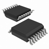
NE1617ADS,112 NXP Semiconductors, NE1617ADS,112 Datasheet - Page 6

NE1617ADS,112
Manufacturer Part Number
NE1617ADS,112
Description
IC TEMP MONITOR 16SSOP
Manufacturer
NXP Semiconductors
Datasheet
1.NE1617ADS118.pdf
(27 pages)
Specifications of NE1617ADS,112
Function
Temp Monitoring System (Sensor)
Topology
ADC, Multiplexer, Register Bank
Sensor Type
External & Internal
Sensing Temperature
-55°C ~ 125°C, External Sensor
Output Type
SMBus™
Output Alarm
Yes
Output Fan
No
Voltage - Supply
3 V ~ 5.5 V
Operating Temperature
-55°C ~ 125°C
Mounting Type
Surface Mount
Package / Case
16-QSOP
Temperature Sensor Function
Temp Sensor
Interface Type
Serial (2-Wire)
Operating Temperature (min)
0C
Operating Temperature (max)
125C
Operating Temperature Classification
Military
Operating Supply Voltage (min)
3V
Operating Supply Voltage (typ)
3.3/5V
Operating Supply Voltage (max)
5.5V
Lead Free Status / RoHS Status
Lead free / RoHS Compliant
Other names
935268119112
NE1617ADS
NE1617ADS
NE1617ADS
NE1617ADS
NXP Semiconductors
8. Temperature monitor with SMBus serial interface
NE1617A_4
Product data sheet
7.2 No calibration is required
7.3 Address logic
8.1 Serial bus interface
8.2 Slave address
than 3300 pF) connected between D+ and D is recommended. Capacitance higher than
3300 pF will introduce measurement error due to the rise time of the switched current
source.
As mentioned in
10 : 1 ratio to measure the forward voltage of the diode (V
the diode saturation current (a heavily process and temperature dependent variable), and
results in the forward voltage being proportional to absolute temperature.
The address pins of the NE1617A can be forced into one of three levels: LOW (GND),
HIGH (V
address pins at the starting of every conversion, it is suggested that those address pins
should be hard-wired to the logic applied, so that the logic is consistently existed at the
address pins. During the address sensing period, the device forces a current at each
address pin and compares the voltage developed across the external connection with the
predefined threshold voltage in order to define the logic level. If an external resistor is
used for the connection of the address, then its value should be less than 2 k to prevent
the error in logic detection from happening. Resistors of 1 k are recommended.
The device can be connected to a standard 2-wire serial interface System Management
Bus (SMBus) as a slave device under the control of a master device, using two device
terminals SCLK and SDATA. The operation of the device to the bus is described with
details in the following sections.
The device address is defined by the logical connections applied to the device pins ADD0
and ADD1. A list of selectable addresses are shown in
be set to any one of those nine combinations and more than one device can reside on the
same bus without address conflict. Note that the state of the device address pins is
sampled and latched not only at power-up step, but also at starting point of every
conversion.
Table 3.
n.c. = not connected
ADD0
GND
GND
GND
n.c.
n.c.
n.c.
[1]
DD
Device slave address
), or ‘not connected’ (n.c.). Because the NE1617A samples and latches the
ADD1
GND
n.c.
V
GND
n.c.
V
DD
DD
Section
[1]
Rev. 04 — 30 July 2009
7.1, the NE1617A uses two well-controlled current sources of
Address byte
0011 000
0011 001
0011 010
0101 001
0101 010
0101 011
Temperature monitor for microprocessor systems
Table
BE
). This technique eliminates
3. The device address can
NE1617A
© NXP B.V. 2009. All rights reserved.
6 of 27


