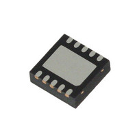
L6728AHTR STMicroelectronics, L6728AHTR Datasheet - Page 5

L6728AHTR
Manufacturer Part Number
L6728AHTR
Description
IC CTLR PWM SGL PHASE 10-VFQFPN
Manufacturer
STMicroelectronics
Datasheet
1.L6728AHTR.pdf
(33 pages)
Specifications of L6728AHTR
Pwm Type
Voltage Mode
Number Of Outputs
1
Frequency - Max
660kHz
Duty Cycle
67%
Voltage - Supply
5 V ~ 12 V
Buck
Yes
Boost
No
Flyback
No
Inverting
No
Doubler
No
Divider
No
Cuk
No
Isolated
No
Operating Temperature
-40°C ~ 125°C
Package / Case
10-VFQFN, 10-VFQFPN
Frequency-max
660kHz
Lead Free Status / RoHS Status
Lead free / RoHS Compliant
Other names
497-8977-2
Available stocks
Company
Part Number
Manufacturer
Quantity
Price
Company:
Part Number:
L6728AHTR
Manufacturer:
PHI
Quantity:
1 800
Company:
Part Number:
L6728AHTR
Manufacturer:
STMicroelectronics
Quantity:
10 000
Part Number:
L6728AHTR
Manufacturer:
ST
Quantity:
20 000
L6728AH
2
2.1
Table 2.
Pin #
10
1
2
3
4
5
6
7
8
9
LGATE / OC
COMP / DIS
PGOOD
PHASE
UGATE
BOOT
Name
VSEN
GND
VCC
FB
Pins description and connection diagrams
Figure 3.
Pin descriptions
Pin description
HS driver supply.
Connect through a capacitor (100 nF) to the floating node (LS-Drain) pin and provide
necessary bootstrap diode from V
HS driver return path, current-reading and adaptive-dead-time monitor. Connect to the LS
drain to sense R
adaptive-dead-time control circuitry to monitor when HS MOSFET is OFF.
HS driver output. Connect directly to HS MOSFET gate.
LGATE. LS driver output. Connect directly to LS MOSFET gate.
OC over-current threshold set. During a short period of time following V
threshold, a 10 μA current is sourced from this pin. Connect to GND with an R
greater than 5 kΩ to program OC Threshold. The resulting voltage at this pin is sampled and
held internally as the OC set point. Maximum programmable OC threshold is 0.55 V. A voltage
greater than 0.6 V activates an internal clamp and causes OC threshold to be set at the
maximum value.
All internal references, logic and drivers are connected to this pin.
Connect to the PCB ground plane.
Device and drivers power supply.
Operative range from 5 V to 12 V. Filter with at least 1 μF MLCC to GND.
COMP. Error amplifier output. Connect with an R
control loop.
DIS. The device can be disabled by pushing this pin lower than 0.75 V (typ). Setting free the
pin, the device enables again.
Error amplifier inverting input.
Connect with a resistor R
used to regulate voltages higher than the reference.
Regulated voltage sense pin for OVP and UVP protections and PGOOD. Connect to the
output regulated voltage, or to the output resistor divider if the regulated voltage is higher than
the reference.
Open drain output set free after SS has finished and pulled low when VSEN is outside the
relative window. Pull up to a voltage equal or lower than V
Pins connection (top view)
DS(on)
LGATE / OC
PHASE
UGATE
drop to measure the output current. This pin is also used by the
BOOT
FB
GND
Doc ID 15726 Rev 1
to the output regulated voltage. Output resistor divider may be
CC
1
2
3
4
5
.
L6728A
L6728AH
Function
Pins description and connection diagrams
F
10
- C
9
8
7
6
F
// C
PGOOD
VSEN
FB
COMP / DIS
VCC
CC
P
. If not used it can be left floating.
to FB to compensate the device
CC
rising over UVLO
OCSET
resistor
5/33


