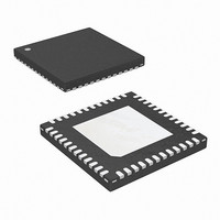
ISL9502CRZ Intersil, ISL9502CRZ Datasheet - Page 5

ISL9502CRZ
Manufacturer Part Number
ISL9502CRZ
Description
IC CTRLR PWM 2PHASE GPU 48-QFN
Manufacturer
Intersil
Datasheet
1.ISL9502CRZ-T.pdf
(24 pages)
Specifications of ISL9502CRZ
Pwm Type
Controller
Number Of Outputs
1
Frequency - Max
500kHz
Voltage - Supply
4.75 V ~ 5.25 V
Buck
Yes
Boost
No
Flyback
No
Inverting
No
Doubler
No
Divider
No
Cuk
No
Isolated
No
Operating Temperature
-10°C ~ 100°C
Package / Case
48-VQFN
Frequency-max
500kHz
Lead Free Status / RoHS Status
Lead free / RoHS Compliant
Duty Cycle
-
Electrical Specifications
ISL9502 Gate Driver Timing Diagram
Functional Pin Description
PGOOD - Power good open-drain output. Will be pulled up
externally by a 680Ω resistor to VCCP or 1.9kΩ to 3.3V.
SET3 - Low load current indicator input. When asserted low,
indicates a reduced load-current condition, and product goes
into single phase operation.
VDD - 5V control power supply.
RBIAS - 147kΩ resistor to GND sets internal current
reference.
VRHOT# - Thermal overload output indicator with
open-drain output. Over- temperature pull-down resistance
is 10Ω.
NTC - Thermistor input to VRHOT# circuit and a 60µA
current source is connected internally to this pin.
SOFT - A capacitor from this pin to GND pin sets the
maximum slew rate of the output voltage. The SOFT pin is
the non-inverting input of the error amplifier.
Leakage Current of SET1
DAC(VSEL0-VSEL5), SET3 and
SET2 Inputs Low
DAC(VSEL0-VSEL5), SET3 and
SET2 Inputs High
Leakage Current of DAC(VSEL0-
VSEL5), SET3 and SET2
THERMAL MONITOR
NTC Source Current
Over-temperature Threshold
VRHOT# Low Output Resistance
PARAMETER
UGATE
LGATE
PWM
t
FL
5
V
DD
1V
t
PDHU
= 5V, T
SYMBOL
I
I
IH_SET1
IL_SET1
R
V
V
I
HOT
I
IH
IL
IH
IL
A
= -10°C to 100°C, Unless Otherwise Specified. (Continued)
t
RU
SET1 input is low
SET1 input is high at 3.3V
Logic input is low
Logic input is high at 1V
NTC = 1.3 V
V(NTC) falling
I = 20mA
ISL9502
TEST CONDITIONS
1V
t
PDHL
t
FU
OCSET - Over-current set input. A resistor from this pin to
VO sets DROOP voltage limit for OC trip. A 10µA current
source is connected internally to this pin.
VW - A resistor from this pin to COMP programs the
switching frequency (exa. 4.42kΩ ≅ 300kHz).
COMP - This pin is the output of the error amplifier.
FB - This pin is the inverting input of error amplifier.
FB2 - There is a switch between FB2 pin and the FB pin.
The switch is closed in single-phase operation and is
opened in two phase operation. The components connecting
to FB2 is to adjust the compensation in single phase
operation to achieve optimum performance if needed.
VDIFF - This pin is the output of the differential amplifier.
VSEN - Remote core voltage sense input.
RTN - Remote core voltage sense return.
t
RL
1.165
MIN
0.7
53
-1
-1
-
-
-
-
TYP
0.45
0.45
1.18
60
0
0
5
-
-
MAX
0.3
1.2
67
1
1
9
-
-
-
July 17, 2006
UNITS
FN9275.1
µA
µA
µA
µA
µA
V
V
V
Ω


