ISL85001IRZ Intersil, ISL85001IRZ Datasheet - Page 14
ISL85001IRZ
Manufacturer Part Number
ISL85001IRZ
Description
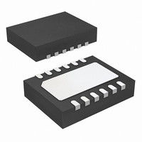
IC REG PWM BUCK 1A 12-DFN
Manufacturer
Intersil
Type
Step-Down (Buck), PWM - Voltage Moder
Datasheet
1.ISL85001IRZ-T.pdf
(15 pages)
Specifications of ISL85001IRZ
Internal Switch(s)
Yes
Synchronous Rectifier
No
Number Of Outputs
1
Voltage - Output
0.6 ~ 19 V
Current - Output
1A
Frequency - Switching
500kHz
Voltage - Input
4.5 ~ 25 V
Operating Temperature
-40°C ~ 85°C
Mounting Type
*
Package / Case
12-DFN
Voltage - Supply
4.5 V ~ 25 V
Frequency-max
550kHz
Duty Cycle
80%
Pwm Type
Voltage Mode
Buck
Yes
Boost
No
Flyback
No
Inverting
No
Doubler
No
Divider
No
Cuk
No
Isolated
No
Lead Free Status / RoHS Status
Lead free / RoHS Compliant
Available stocks
Company
Part Number
Manufacturer
Quantity
Price
Company:

Part Number:
ISL85001IRZ
Manufacturer:
Intersil
Quantity:
150


A more detailed explanation of voltage mode control of a
buck regulator can be found in TB417, entitled “Designing
Stable Compensation Networks for Single Phase Voltage
Mode Buck Regulators.”
http://www.intersil.com/data/tb/tb417.pdf
Layout Considerations
Layout is very important in high frequency switching
converter design. With power devices switching efficiently
between 100kHz and 600kHz, the resulting current
transitions from one device to another cause voltage spikes
across the interconnecting impedances and parasitic circuit
elements. These voltage spikes can degrade efficiency,
radiate noise into the circuit, and lead to device overvoltage
stress. Careful component layout and printed circuit board
design minimizes these voltage spikes.
As an example, consider the turn-off transition of the upper
MOSFET. Prior to turn-off, the MOSFET is carrying the full load
current. During turn-off, current stops flowing in the MOSFET
and is picked up by the Schottky diode. Any parasitic
inductance in the switched current path generates a large
voltage spike during the switching interval. Careful component
selection, tight layout of the critical components, and short, wide
traces minimizes the magnitude of voltage spikes.
There are two sets of critical components in the ISL85001
switching converter. The switching components are the most
critical because they switch large amounts of energy, and
therefore tend to generate large amounts of noise. Next are
the small signal components, which connect to sensitive
nodes or supply critical bypass current and signal coupling.
A multi-layer printed circuit board is recommended. Figure 23
shows the connections of the critical components in the
converter. Note that capacitors C
represent numerous physical capacitors. Dedicate one solid
layer, usually a middle layer of the PC board, for a ground
plane and make all critical component ground connections
with vias to this layer. Dedicate another solid layer as a power
plane and break this plane into smaller islands of common
voltage levels. Keep the metal runs from the PHASE terminals
to the output inductor short. The power plane should support
the input power and output power nodes. Use copper filled
polygons on the top and bottom circuit layers for the phase
nodes. Use the remaining printed circuit layers for small signal
wiring.
In order to dissipate heat generated by the internal LDO and
MOSFET, the ground pad, pin 13, should be connected to
the internal ground plane through at least four vias. This
allows the heat to move away from the IC and also ties the
pad to the ground plane through a low impedance path.
The switching components should be placed close to the
ISL85001 first. Minimize the length of the connections
between the input capacitors, C
by placing them nearby. Position both the ceramic and bulk
14
IN
IN
, and the power switches
and C
OUT
could each
ISL85001
input capacitors as close to the upper MOSFET drain as
possible. Position the output inductor and output capacitors
between the upper and Schottky diode and the load.
The critical small signal components include any bypass
capacitors, feedback components, and compensation
components. Place the PWM converter compensation
components close to the FB and COMP pins. The feedback
resistors should be located as close as possible to the FB
pin with vias tied straight to the ground plane as required.
5V
C
FIGURE 23. PRINTED CIRCUIT BOARD POWER PLANES AND
BP1
KEY
ISLAND ON POWER PLANE LAYER
ISLAND ON CIRCUIT AND/OR POWER PLANE LAYER
VIA CONNECTION TO GROUND PLANE
VDD
ISLANDS
GND PAD
ISL85001
PHASE
COMP
GND
VIN
FB
V
IN
R
D
C
2
2
R
4
C
L
IN
C
C
1
OUT1
C
3
R
1
R
3
V
March 17, 2009
OUT1
FN6769.1
Related parts for ISL85001IRZ
Image
Part Number
Description
Manufacturer
Datasheet
Request
R

Part Number:
Description:
2a Standard Buck Pwm Regulator
Manufacturer:
Intersil Corporation
Datasheet:
Part Number:
Description:
Intersil Corporation [CMOS Serial Controller Interface]
Manufacturer:
Intersil Corporation
Datasheet:
Part Number:
Description:
Manufacturer:
Intersil Corporation
Datasheet:
Part Number:
Description:
357-036-542-201 CARDEDGE 36POS DL .156 BLK LOPRO
Manufacturer:
Intersil Corporation
Datasheet:
Part Number:
Description:
1024-Word x 4-Bit LSI Static RAM
Manufacturer:
Intersil Corporation
Datasheet:
Part Number:
Description:
General Purpose NPN Transistor Arrays FN341.4
Manufacturer:
Intersil Corporation
Datasheet:
Part Number:
Description:
CMOS 16-Bit Microprocessor
Manufacturer:
Intersil Corporation
Datasheet:
Part Number:
Description:
Manufacturer:
Intersil Corporation
Datasheet:
Part Number:
Description:
Manufacturer:
Intersil Corporation
Datasheet:
Part Number:
Description:
Manufacturer:
Intersil Corporation
Datasheet:
Part Number:
Description:
Manufacturer:
Intersil Corporation
Datasheet:
Part Number:
Description:
CMOS 6-Bit Latch and Decoder Memory Interfaces
Manufacturer:
Intersil Corporation
Datasheet:
Part Number:
Description:
CA3046General Purpose NPN Transistor Arrays
Manufacturer:
Intersil Corporation
Datasheet:
Part Number:
Description:
Manufacturer:
Intersil Corporation
Datasheet:
Part Number:
Description:
TR909 DLC/FLC SLIC with Low Power Standby
Manufacturer:
Intersil Corporation
Datasheet: