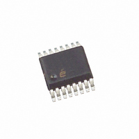
ISL6742AAZA-T Intersil, ISL6742AAZA-T Datasheet - Page 13

ISL6742AAZA-T
Manufacturer Part Number
ISL6742AAZA-T
Description
IC CTRLR PWM DBL ENDED 16-QSOP
Manufacturer
Intersil
Datasheet
1.ISL6742AAZA.pdf
(18 pages)
Specifications of ISL6742AAZA-T
Pwm Type
Voltage/Current Mode
Number Of Outputs
4
Frequency - Max
2MHz
Duty Cycle
100%
Voltage - Supply
9 V ~ 16 V
Buck
No
Boost
No
Flyback
No
Inverting
No
Doubler
No
Divider
No
Cuk
No
Isolated
No
Operating Temperature
-40°C ~ 105°C
Package / Case
16-QSOP
Frequency-max
2MHz
Lead Free Status / RoHS Status
Lead free / RoHS Compliant
Other names
ISL6742AAZA-TTR
Available stocks
Company
Part Number
Manufacturer
Quantity
Price
Company:
Part Number:
ISL6742AAZA-T
Manufacturer:
Intersil
Quantity:
2 000
Part Number:
ISL6742AAZA-T
Manufacturer:
INTERSIL
Quantity:
20 000
Synchronous Rectifier Outputs and Control
The ISL6742 provides double-ended PWM outputs, OUTA
and OUTB, and synchronous rectifier (SR) outputs, OUTAN
and OUTBN. The SR outputs are the complements of the
PWM outputs. It should be noted that complemented outputs
are used in conjunction with the opposite PWM output, i.e.
OUTA and OUTBN are paired together and OUTB and
OUTAN are paired together.
Referring to Figure 11, the SRs alternate between being both
on during the free-wheeling portion of the cycle
(OUTA/OUTB off), and one or the other being off when
OUTA or OUTB is on. If OUTA is on, its corresponding SR
must also be on, indicating that OUTBN is the correct SR
control signal. Likewise, if OUTB is on, its corresponding SR
must also be on, indicating that OUTAN is the correct SR
control signal.
A useful feature of the ISL6742 is the ability to vary the
phase relationship between the PWM outputs (OUTA,
OUTB) and their complements (OUTAN, OUTBN) by
±300ns. This feature allows the designer to compensate for
differences in the signal propagation delays between the
PWM FETs and the SR FETs. A voltage applied to VADJ
controls the phase relationship. Figures 12 and 13
demonstrate the delay relationships.
OUTAN
OUTBN
OUTA
OUTB
(SR1)
(SR2)
CT
FIGURE 11. BASIC WAVEFORM TIMING
13
ISL6742
Setting VADJ to VREF/2 results in no delay on any output.
The no delay voltage has a ±75mV tolerance window.
Control voltages below the VREF/2 zero delay threshold
cause the PWM outputs, OUTA/OUTB, to be delayed.
Control voltages greater than the VREF/2 zero delay
threshold cause the SR outputs, OUTAN/OUTBN, to be
delayed. It should be noted that when the PWM outputs,
OUTA/OUTB, are delayed, the CS to output propagation
delay is increased by the amount of the added delay.
The delay feature is provided to compensate for mismatched
propagation delays between the PWM and SR outputs as
may be experienced when one set of signals crosses the
primary-secondary isolation boundary. If required, individual
output pulses may be stretched or compressed as required
using external resistors, capacitors, and diodes.
FIGURE 13. WAVEFORM TIMING WITH SR OUTPUTS
FIGURE 12. WAVEFORM TIMING WITH PWM OUTPUTS
OUTAN
OUTBN
OUTAN
OUTBN
OUTA
OUTB
(SR1)
(SR2)
OUTA
OUTB
(SR1)
(SR2)
CT
CT
DELAYED, 2.575V < VADJ < 5.00V
DELAYED, 0V < VADJ < 2.425V
October 31, 2008
FN9183.2


