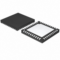
ISL6326BIRZ-T Intersil, ISL6326BIRZ-T Datasheet - Page 18

ISL6326BIRZ-T
Manufacturer Part Number
ISL6326BIRZ-T
Description
IC CTRLR PWM 4PHASE BUCK 40-QFN
Manufacturer
Intersil
Datasheet
1.ISL6326BCRZ.pdf
(30 pages)
Specifications of ISL6326BIRZ-T
Pwm Type
Voltage Mode
Number Of Outputs
1
Frequency - Max
275kHz
Duty Cycle
25%
Voltage - Supply
4.75 V ~ 5.25 V
Buck
Yes
Boost
No
Flyback
No
Inverting
No
Doubler
No
Divider
No
Cuk
No
Isolated
No
Operating Temperature
-40°C ~ 85°C
Package / Case
40-VFQFN, 40-VFQFPN
Frequency-max
275kHz
Lead Free Status / RoHS Status
Lead free / RoHS Compliant
Load-Line Regulation
Some microprocessor manufacturers require a precisely-
controlled output resistance. This dependence of output
voltage on load current is often termed “droop” or “load line”
regulation. By adding a well controlled output impedance,
the output voltage can effectively be level shifted in a
direction which works to achieve the load-line regulation
required by these manufacturers.
In other cases, the designer may determine that a more
cost-effective solution can be achieved by adding droop.
Droop can help to reduce the output-voltage spike that
results from fast load-current demand changes.
The magnitude of the spike is dictated by the ESR and ESL
of the output capacitors selected. By positioning the no-load
voltage level near the upper specification limit, a larger
negative spike can be sustained without crossing the lower
limit. By adding a well controlled output impedance, the
output voltage under load can effectively be level shifted
down so that a larger positive spike can be sustained without
crossing the upper specification limit.
As shown in Figure 5, a current proportional to the average
current of all active channels, I
load-line regulation resistor R
across R
creating an output voltage droop with a steady-state value
defined as
The regulated output voltage is reduced by the droop voltage
V
derived by combining Equation 8 with the appropriate
sample current expression defined by the current sense
method employed.
Where V
programmed offset voltage, I
of the converter, R
the ISEN+ pin, and R
active channel number, and R
depending on the sensing method.
Therefore the equivalent loadline impedance, i.e. Droop
impedance, is equal to:
V
V
R
DROOP
DROOP
OUT
LL
=
=
------------
R
. The output voltage as a function of load current is
N
FB
REF
V
FB
=
REF
I
is proportional to the output current, effectively
----------------- -
R
AVG
is the reference voltage, V
ISEN
R
–
X
V
R
OFS
ISEN
FB
FB
–
⎛
⎜
⎝
is the sense resistor connected to
I
---------------- -
is the feedback resistor, N is the
LOAD
N
LOAD
18
FB
X
AVG
----------------- - R
R
is the DCR, or R
. The resulting voltage drop
ISEN
R
, flows from FB through a
X
is the total output current
FB
OFS
⎞
⎟
⎠
is the
SENSE
(EQ. 10)
(EQ. 8)
(EQ. 9)
ISL6326B
Output-Voltage Offset Programming
The ISL6326B allows the designer to accurately adjust the
offset voltage. When a resistor, R
OFS to VCC, the voltage across it is regulated to 1.6V. This
causes a proportional current (I
R
regulated to 0.4V, and I
between DAC and REF, R
product (I
These functions are shown in Figure 6.
Once the desired output offset voltage has been determined,
use the following formulas to set R
For Positive Offset (connect R
For Negative Offset (connect R
R
R
OFS
OFS
OFS
FIGURE 6. OUTPUT VOLTAGE OFFSET PROGRAMMING
is connected to ground, the voltage across it is
=
=
1.6
----------------------------- -
0.4
----------------------------- -
OFS
V
V
1.6V
OFFSET
OFFSET
×
×
R
R
VCC
x R
+
-
REF
REF
OFS
0.4V
E/A
) is equal to the desired offset voltage.
OFS
GND
+
-
REF
FB
flows out of OFS. A resistor
, is selected so that the
OFS
OFS
OFS
OFS
OFS
to VCC):
DYNAMIC
) to flow into OFS. If
to GND):
VID D/A
, is connected between
:
ISL6326B
April 21, 2006
DAC
OFS
GND
VCC
OR
(EQ. 12)
(EQ. 11)
FN9286.0
REF
R
R
C
REF
REF
OFS


