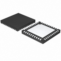
ISL6564ACRZ-T Intersil, ISL6564ACRZ-T Datasheet - Page 11

ISL6564ACRZ-T
Manufacturer Part Number
ISL6564ACRZ-T
Description
IC CTRLR PWM MULTIPHASE 40-QFN
Manufacturer
Intersil
Datasheet
1.ISL6564ACRZ.pdf
(28 pages)
Specifications of ISL6564ACRZ-T
Pwm Type
Voltage Mode
Number Of Outputs
1
Frequency - Max
1.5MHz
Duty Cycle
66.7%
Voltage - Supply
4.75 V ~ 5.25 V
Buck
Yes
Boost
No
Flyback
No
Inverting
No
Doubler
No
Divider
No
Cuk
No
Isolated
No
Operating Temperature
0°C ~ 70°C
Package / Case
40-VFQFN, 40-VFQFPN
Frequency-max
1.5MHz
Lead Free Status / RoHS Status
Lead free / RoHS Compliant
PGOOD
PGOOD is used as an indication of the end of soft-start per
the microprocessor specification. It is an open-drain logic
output that is low impedance until the soft-start is completed.
It will be pulled low again once the undervoltage point is
reached.
OFS
The OFS pin provides a means to program a DC offset
current for generating a DC offset voltage at the REF input.
The offset current is generated via an external resistor and
precision internal voltage references. The polarity of the
offset is selected by connecting the resistor to GND or VCC.
For no offset, the OFS pin should be left unterminated.
OVP
Overvoltage protection pin. This pin pulls to VCC and is
latched when an overvoltage condition is detected. Connect
this pin to the gate of an SCR or MOSFET tied from V
V
be pulled above VCC as high as 15V to ground with an
external resistor. However, it is only capable of pulling low
when VCC is above 2V.
DRVEN
Driver enable pin. This pin can be used to enable the drivers
which have enable pins such as ISL6605 or ISL6608. If
ISL6564A is used with Intersil ISL6612 drivers, it’s not
necessary to use this pin.
IDROOP and IOUT
IDROOP and IOUT are the output pins of sensed average
channel current which is proportional to load current. They
are designed for flexible application purposes.
In the application which does not require loadline, leave
IDROOP pin open. In the application which requires load
line, connect IDROOP pin to FB so that the sensed average
current will flow through the resistor between FB and VDIFF
to create a voltage drop which is proportional to load current.
IOUT is typically used for load current indication.
Operation
Multiphase Power Conversion
Microprocessor load current profiles have changed to the
point that the advantages of multiphase power conversion
are impossible to ignore. The technical challenges
associated with producing a single-phase converter which is
both cost-effective and thermally viable have forced a
change to the cost-saving approach of multiphase. The
ISL6564A controller helps reduce the complexity of
implementation by integrating vital functions and requiring
minimal output components. The block diagrams on pages
3, 4, 5, 6, and 7 provide top level views of multiphase power
conversion using the ISL6564A controller.
OUT
to ground to prevent damage to the load. This pin may
11
IN
or
ISL6564A
Interleaving
The switching of each channel in a multiphase converter is
timed to be symmetrically out of phase with each of the other
channels. In a 3-phase converter, each channel switches 1/3
cycle after the previous channel and 1/3 cycle before the
following channel. As a result, the three-phase converter has
a combined ripple frequency three times greater than the
ripple frequency of any one phase. In addition, the peak-to-
peak amplitude of the combined inductor currents is reduced
in proportion to the number of phases (Equations 1 and 2).
Increased ripple frequency and lower ripple amplitude mean
that the designer can use less per-channel inductance and
lower total output capacitance for any performance
specification.
Figure 1 illustrates the multiplicative effect on output ripple
frequency. The three channel currents (IL1, IL2, and IL3)
combine to form the AC ripple current and the DC load
current. The ripple component has three times the ripple
frequency of each individual channel current. Each PWM
pulse is terminated 1/3 of a cycle after the PWM pulse of the
previous phase. The peak-to-peak current for each phase is
about 7A, and the DC components of the inductor currents
combine to feed the load.
To understand the reduction of ripple current amplitude in the
multiphase circuit, examine the equation representing an
individual channel’s peak-to-peak inductor current.
In Equation 1, V
voltages respectively, L is the single-channel inductor value,
and f
I
PP
FIGURE 1. PWM AND INDUCTOR-CURRENT WAVEFORMS
=
S
(
----------------------------------------------------- -
V
is the switching frequency.
IN
PWM1, 5V/DIV
–
L f
V
IL1 + IL2 + IL3, 7A/DIV
FOR 3-PHASE CONVERTER
OUT
S
V
IN
IL1, 7A/DIV
IN
) V
and V
OUT
PWM3, 5V/DIV
OUT
1µs/DIV
are the input and output
IL3, 7A/DIV
PWM2, 5V/DIV
IL2, 7A/DIV
March 20, 2007
FN6285.1
(EQ. 1)


