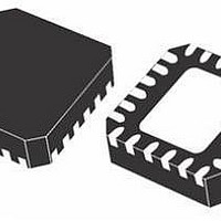
PM6641TR STMicroelectronics, PM6641TR Datasheet - Page 40

PM6641TR
Manufacturer Part Number
PM6641TR
Description
IC CTLR DDR2/3 MONO VR 48VFQFPN
Manufacturer
STMicroelectronics
Datasheet
1.PM6641TR.pdf
(47 pages)
Specifications of PM6641TR
Applications
Converter, DDR2, DDR3
Voltage - Input
2.7 ~ 5.5 V
Number Of Outputs
3
Voltage - Output
0.8 ~ 5.5 V
Operating Temperature
0°C ~ 85°C
Mounting Type
Surface Mount
Package / Case
48-VFQFN
For Use With
497-8425 - KIT EVAL PM6641 CHIPSET/DDR2/3
Lead Free Status / RoHS Status
Lead free / RoHS Compliant
Other names
497-6893-2
PM6641TR
PM6641TR
Available stocks
Company
Part Number
Manufacturer
Quantity
Price
Company:
Part Number:
PM6641TR
Manufacturer:
STM
Quantity:
35 839
Components selection
8.5
40/47
Layout guidelines
Each signal is referred to AGND, the analog ground. In a typical 4-layers PCB one internal
layer should be dedicated to this common ground. The IC thermal pad must be connected to
AGND plane through multiple VIAs, in order to remove the IC heat and to obtain the best
performance. Furthermore, each switching regulator has a dedicated power ground
(SGND_1Sxx); all these SGNDs must be star-connected, in a single point, with AGND.
For each switching section the power components (inductor and input/output capacitors)
must be placed near the VSW_1Sxx, VIN_1Sxx and SGND_1Sxx pins and connected with
large (at least 20 mils or larger) and short PCB traces, in order to limit the path of the current
high frequency components and, consequently, to reduce the injected noise. If the power
components routing involves more than one layer, as many VIAs as possible must be
inserted to reduce the series resistance and improve the global efficiency.
The VTT external components (input and output capacitors) must be placed near the LDO
regulator input (LDOIN) and output (VTT) pins, and must be routed with large and short
traces, in order to limit the parasitic series resistance.
The feedback pins (VFB_1Sxx and VTTFB) must reach the feedback points through
dedicated PCB traces, typically 10 mils width; larger feedback traces are not required.
For reference layout, refer to PM6641 demonstration kit document.
Doc ID 13510 Rev 3
PM6641


