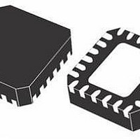
PM6641 STMicroelectronics, PM6641 Datasheet - Page 22

PM6641
Manufacturer Part Number
PM6641
Description
IC MONO VR DDR2/3 PC VFQFPN-48
Manufacturer
STMicroelectronics
Datasheet
1.PM6641TR.pdf
(47 pages)
Specifications of PM6641
Applications
Converter, DDR2, DDR3
Voltage - Input
2.7 ~ 5.5 V
Number Of Outputs
3
Voltage - Output
0.8 ~ 5.5 V
Operating Temperature
0°C ~ 85°C
Mounting Type
Surface Mount
Package / Case
48-VFQFN
Output Voltage
0.9 V
Output Current
3 A
Input Voltage
2.7 V to 5.5 V
Switching Frequency
1000 KHz
Operating Temperature Range
- 40 C to + 125 C
Mounting Style
SMD/SMT
For Use With
497-8425 - KIT EVAL PM6641 CHIPSET/DDR2/3
Lead Free Status / RoHS Status
Lead free / RoHS Compliant
Available stocks
Company
Part Number
Manufacturer
Quantity
Price
Company:
Part Number:
PM6641
Manufacturer:
BITECHNOL
Quantity:
2 000
Part Number:
PM6641
Manufacturer:
ST
Quantity:
20 000
Company:
Part Number:
PM6641TR
Manufacturer:
STM
Quantity:
35 839
Device description
7.1.4
7.2
22/47
S3 and S5 power management pins
According to DDR2/3 memories supply requirements, the PM6641 can manage all S0 to S5
system states just connecting EN_VTT – EN_1S8 pins to their respective sleep-mode
signals in the notebook’s motherboard: connect EN_1S8 to S5 and EN_VTT to S3.
Keeping EN_VTT and EN_1S8 high, the S0 (full-on) state is decoded and the outputs are
alive.
In S3 state (EN_1S8 = 1, EN_VTT = 0), the PM6641 maintains VDDQ and VTTREF outputs
active and VTT output in high-impedance as needed.
In S4/S5 states (EN_1S8 = EN_VTT = 0) all outputs are turned off and, according to DSCG
pin voltage, the proper Soft-End is performed (see
page 29
The following table resumes the DDR power supply states.
Table 8.
Chipset supply
The chipset power supply section is based on two constant frequency current-mode buck
regulators with a pre-fixed output voltage of 1.5 V and 1.05 V.
These two independent rails have programmable switching frequency, set by inserting an
external resistor between SET_SWF pin and AGND. The PM6641 allows also to manage
the switching regulators phases for 1.5 V, 1.05 V and 1.8 V (VDDQ) rails in order to limit the
RMS input current (see
Chapter 7.9: Phase management on page 30
The output voltages can easily be set to the pre-fixed value by connecting the feedback pins
VFB_1S5 and VFB_1S05 directly to the respective output rail, avoiding the use of external
components. However, if a different output voltage is desired, the feedback pins can be
independently connected to the central tap of a resistor divider.
The output voltage can be adjusted from 0.8 V up to the input voltage value, decreased by a
drop due to the high-side MOSFET on resistance.
(see
Both regulators are current-mode step-down switching regulators whose control loop needs
to be compensated by inserting a resistor-capacitor series connected between the
compensation pin (COMP_1S5 and COMP_1S05) and ground; if electrolytic capacitor with
relevant equivalent series resistance (ESR) are used, an additional capacitor between this
compensation pin and ground can be useful (see
on page 24
S3 (EN_VTT) S5 (EN_1S8)
Chapter 7.5: Output voltage divider on page 27
1
0
0
section for details).
section for details). The classical slope compensation, which allows the peak
S3 and S5 sleep-states decoding
1
1
0
Chapter 7.8: Switching frequency selection on page 29
(Suspend-to-RAM)
(Suspend-to-disk)
System state
Doc ID 13510 Rev 3
(Full-on)
S4/S5
S0
S3
section for details).
Off (Discharge) Off (Discharge) Off (Discharge)
Chapter 7.3: SW regulators control loop
VDDQ
Chapter 7.7: Outputs soft-end on
On
On
section for details).
VTTREF
On
On
and
VTT
Hi-Z
On
PM6641


