ISL6265HRTZ Intersil, ISL6265HRTZ Datasheet - Page 20
ISL6265HRTZ
Manufacturer Part Number
ISL6265HRTZ
Description
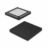
IC CTLR MULTI-OUTPUT 48-TQFN
Manufacturer
Intersil
Datasheet
1.ISL6265HRTZ.pdf
(24 pages)
Specifications of ISL6265HRTZ
Applications
Controller, AMD SVI Capable Mobile
Voltage - Input
5 ~ 24 V
Number Of Outputs
3
Voltage - Output
0.5 ~ 1.55 V
Operating Temperature
-10°C ~ 100°C
Mounting Type
Surface Mount
Package / Case
48-TQFN
Lead Free Status / RoHS Status
Lead free / RoHS Compliant
Available stocks
Company
Part Number
Manufacturer
Quantity
Price
Company:

Part Number:
ISL6265HRTZ
Manufacturer:
MAXIM
Quantity:
24


PWM outputs turn off both Core and Northbridge internal
drivers and PGOOD goes low.
General Application Design Guide
This design guide is intended to provide a high-level
explanation of the steps necessary to design a single-phase
power converter. It is assumed that the reader is familiar with
many of the basic skills and techniques referenced in the
following section. In addition to this guide, Intersil provides
complete reference designs that include schematics, bills of
materials, and example board layouts.
Selecting the LC Output Filter
The output inductor and output capacitor bank form a
low-pass filter responsible for smoothing the pulsating
voltage at the phase node. The output filter also must
support the transient energy required by the load until the
controller can respond. Because it has a low bandwidth
compared to the switching frequency, the output filter limits
the system transient response. The output capacitors must
supply or sink load current while the current in the output
inductors increases or decreases to meet the demand.
The duty cycle of an ideal buck converter is a function of the
input and the output voltage. This relationship is written as
Equation 17:
The output inductor peak-to-peak ripple current is written as
Equation 18:
For this type of application, a typical step-down DC/DC
converter has an I
output load current. The value of I
several criteria such as MOSFET switching loss, inductor
core loss, and the resistive loss of the inductor winding. The
DC copper loss of the inductor can be estimated by
Equation 19:
Where I
The copper loss can be significant so attention must be
given to the DCR selection. Another factor to consider when
choosing the inductor is its saturation characteristics at
elevated temperature. A saturated inductor could cause
destruction of circuit components as well as nuisance OCP
faults.
A DC/DC buck regulator must have output capacitance C
into which ripple current I
a corresponding ripple voltage V
sum of the voltage drop across the capacitor ESR and of the
voltage change stemming from charge moved in and out of
D
I
P
P-P
COPPER
=
---------
V
=
V
IN
O
V
----------------------------- -
LOAD
O
f
SW
•
=
(
1 D
I
•
–
LOAD
is the converter output DC current.
L
)
P-P
2
•
DCR
of 20% to 40% of the maximum DC
P-P
can flow. Current I
20
P-P
P-P
across C
is selected based upon
O,
P-P
which is the
develops
(EQ. 17)
(EQ. 19)
(EQ. 18)
O
ISL6265
the capacitor. These two voltages are written as shown in
Equation 20:
and Equation 21:
If the output of the converter has to support a load with high
pulsating current, several capacitors will need to be paralleled
to reduce the total ESR until the required V
The inductance of the capacitor can cause a brief voltage dip
if the load transient has an extremely high slew rate. Capacitor
ESL can significantly impact output voltage ripple. Low
inductance capacitors should be considered. A capacitor
dissipates heat as a function of RMS current and frequency.
Be sure that I
capacitors so that they operate below the maximum rated
RMS current at F
a capacitor can degrade as much as 50% as the DC voltage
across it increases.
Selection of the Input Capacitor
The input capacitors are responsible for sourcing the AC
component of the input current flowing into the upper
MOSFETs. Their RMS current capability must be sufficient to
handle the AC component of the current drawn by the upper
MOSFETs, which is related to duty cycle and the number of
active phases.
The important parameters for the bulk input capacitance are
the voltage rating and the RMS current rating. For reliable
operation, select bulk capacitors with voltage and current
ratings above the maximum input voltage and capable of
supplying the RMS current required by the switching circuit.
Their voltage rating should be at least 1.25x greater than the
maximum input voltage, while a voltage rating of 1.5x is a
preferred rating. Figure 11 is a graph of the input RMS ripple
current, normalized relative to output load current, as a
function of duty cycle for a single-phase regulator that is
adjusted for converter efficiency.
ΔV
ΔV
ESR
C
=
-----------------------------
8 C
=
•
I
PP
I
O
PP
•
P-P
•
f
E
SW
SR
is shared by a sufficient quantity of paralleled
SW
. Take into account that the rated value of
P-P
is achieved.
May 13, 2009
(EQ. 20)
(EQ. 21)
FN6599.1
Related parts for ISL6265HRTZ
Image
Part Number
Description
Manufacturer
Datasheet
Request
R

Part Number:
Description:
Multi-Output Controller
Manufacturer:
Intersil Corporation
Datasheet:
Part Number:
Description:
Intersil Corporation [CMOS Serial Controller Interface]
Manufacturer:
Intersil Corporation
Datasheet:
Part Number:
Description:
Manufacturer:
Intersil Corporation
Datasheet:
Part Number:
Description:
357-036-542-201 CARDEDGE 36POS DL .156 BLK LOPRO
Manufacturer:
Intersil Corporation
Datasheet:
Part Number:
Description:
1024-Word x 4-Bit LSI Static RAM
Manufacturer:
Intersil Corporation
Datasheet:
Part Number:
Description:
General Purpose NPN Transistor Arrays FN341.4
Manufacturer:
Intersil Corporation
Datasheet:
Part Number:
Description:
CMOS 16-Bit Microprocessor
Manufacturer:
Intersil Corporation
Datasheet:
Part Number:
Description:
Manufacturer:
Intersil Corporation
Datasheet:
Part Number:
Description:
Manufacturer:
Intersil Corporation
Datasheet:
Part Number:
Description:
Manufacturer:
Intersil Corporation
Datasheet:
Part Number:
Description:
Manufacturer:
Intersil Corporation
Datasheet:
Part Number:
Description:
CMOS 6-Bit Latch and Decoder Memory Interfaces
Manufacturer:
Intersil Corporation
Datasheet:
Part Number:
Description:
CA3046General Purpose NPN Transistor Arrays
Manufacturer:
Intersil Corporation
Datasheet:
Part Number:
Description:
Manufacturer:
Intersil Corporation
Datasheet:
Part Number:
Description:
TR909 DLC/FLC SLIC with Low Power Standby
Manufacturer:
Intersil Corporation
Datasheet: