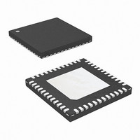
ISL6333ACRZ Intersil, ISL6333ACRZ Datasheet - Page 16

ISL6333ACRZ
Manufacturer Part Number
ISL6333ACRZ
Description
IC CTRLR PWM 3PHASE BUCK 48-QFN
Manufacturer
Intersil
Datasheet
1.ISL6333ACRZ.pdf
(40 pages)
Specifications of ISL6333ACRZ
Applications
Controller, Intel VR11
Voltage - Input
5 ~ 12 V
Number Of Outputs
1
Voltage - Output
0.5 ~ 1.6 V
Operating Temperature
0°C ~ 70°C
Mounting Type
Surface Mount
Package / Case
48-VQFN
Lead Free Status / RoHS Status
Lead free / RoHS Compliant
Available stocks
Company
Part Number
Manufacturer
Quantity
Price
Part Number:
ISL6333ACRZ
Manufacturer:
INTERSIL
Quantity:
20 000
Part Number:
ISL6333ACRZ-T
Manufacturer:
INFINEON/英飞凌
Quantity:
20 000
Functional Pin Descriptions
VCC
VCC is the bias supply for the ICs small-signal circuitry.
Connect this pin to a +5V supply and decouple using a
quality 0.1µF ceramic capacitor.
PVCC1 (ISL6333, ISL6333B Only)
This pin is the input to an internal LDO that regulates the
voltage on the BYP1 pin and should be connected to a +12V
supply. It is very important that this pin is decoupled using a
quality 1.0µF ceramic capacitor.
PVCC2_3 (ISL6333, ISL6333B Only)
This pin is the power supply pin for Channels 2 and 3 lower
MOSFET drivers, and should be connected to a +12V supply.
Decouple this pin with a quality 1.0µF ceramic capacitor.
PVCC1, PVCC2, and PVCC3 (ISL6333A, ISL6333C
Only)
These pins are the power supply pins for Channels 1, 2, and
3 lower MOSFET drivers, and should be connected to a
+12V supply. Decouple these pins with quality 1.0µF
ceramic capacitors
PUVCC
This pin is the power supply pin for Channels 1, 2, and 3
upper MOSFET drivers, and can be connected to any
voltage from +5V to +12V depending on the desired
MOSFET gate-drive level. Decouple this pin with a quality
1.0µF ceramic capacitor.
BYP1 (ISL6333, ISL6333B Only)
This pin is the output of an internal LDO which powers
Channel 1 lower MOSFET driver. A quality 1.0µF ceramic
capacitor should be placed from this pin to ground.
GND
GND is the bias and reference ground for the IC.
EN
This pin is a threshold-sensitive (approximately 0.86V) enable
input for the controllers. Held low, this pin disables controller
operation. Pulled high, the pin enables the controller for
operation.
FS
A resistor, R
switching frequency of the controller. Refer to Equation 46
for proper resistor calculation.
The FS pin also determines whether the controllers operate
in the coupled inductor mode or the standard inductor mode
of operation. Tying the R
controllers to operate in standard inductor mode. Tying the
R
coupled inductor mode.
FS
resistor to VCC sets the controllers to operate in
FS
, tied from this pin to ground sets the channel
FS
resistor to ground will set the
16
ISL6333, ISL6333A, ISL6333B, ISL6333C
VID0, VID1, VID2, VID3, VID4, VID5, VID6, and VID7
These are the inputs for the internal DAC that provide the
reference voltage for output regulation. These pins respond to
TTL logic thresholds. These pins are internally pulled high to
approximately 1.2V, by 40µA internal current sources. The
internal pull-up current decreases to 0 as the VID voltage
approaches the internal pull-up voltage. All VID pins are
compatible with external pull-up voltages not exceeding the
IC’s bias voltage (VCC).
VSEN and RGND
VSEN and RGND are inputs to the precision differential
remote-sense amplifier and should be connected to the sense
pins of the remote load.
VDIFF
VDIFF is the output of the differential remote-sense amplifier.
The voltage on this pin is equal to the difference between
VSEN and RGND.
FB and COMP
These pins are the internal error amplifier inverting input and
output respectively. The FB pin, COMP pin, and the VDIFF
pins are tied together through external R-C networks to
compensate the regulator.
DVC
A series resistor and capacitor can be connected from the
DVC pin to the FB pin to compensate and smooth dynamic
VID transitions.
IDROOP (ISL6333, ISL6333A Only)
The IDROOP pin is the average channel-current sense
output. Connecting this pin directly to FB allows the
converter to incorporate output voltage droop proportional to
the output current. If voltage droop is not desired leave this
pin unconnected.
IMON
The IMON pin is the average channel-current sense output.
This pin is used as a load current indicator to monitor the
output load current.
APA
This is the Adaptive Phase Alignment set pin. A 100µA
current flows into the APA pin and by tying a resistor from
this pin to COMP the trip level for the Adaptive Phase
Alignment circuitry can be set.
REF
The REF input pin is the positive input of the error amplifier. It is
internally connected to the DAC output through a 1kΩ resistor.
A capacitor is used between the REF pin and ground to smooth
the voltage transition during soft-start and Dynamic VID
transitions. This pin can also be bypassed to RGND if desired.
October 8, 2010
FN6520.3


