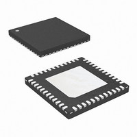
ISL6333ACRZ Intersil, ISL6333ACRZ Datasheet - Page 35

ISL6333ACRZ
Manufacturer Part Number
ISL6333ACRZ
Description
IC CTRLR PWM 3PHASE BUCK 48-QFN
Manufacturer
Intersil
Datasheet
1.ISL6333ACRZ.pdf
(40 pages)
Specifications of ISL6333ACRZ
Applications
Controller, Intel VR11
Voltage - Input
5 ~ 12 V
Number Of Outputs
1
Voltage - Output
0.5 ~ 1.6 V
Operating Temperature
0°C ~ 70°C
Mounting Type
Surface Mount
Package / Case
48-VQFN
Lead Free Status / RoHS Status
Lead free / RoHS Compliant
Available stocks
Company
Part Number
Manufacturer
Quantity
Price
Part Number:
ISL6333ACRZ
Manufacturer:
INTERSIL
Quantity:
20 000
Part Number:
ISL6333ACRZ-T
Manufacturer:
INFINEON/英飞凌
Quantity:
20 000
In Equation 40, L is the per-channel filter inductance divided
by the number of active channels; C is the sum total of all
output capacitors; ESR is the equivalent series resistance of
the bulk output filter capacitance; and V
peak-to-peak sawtooth signal amplitude, as described in the
“Electrical Specifications” on page 13.
Once selected, the compensation values in Equation 40
assure a stable converter with reasonable transient
performance. In most cases, transient performance can be
improved by making adjustments to R
value of R
oscilloscope until no further improvement is noted. Normally,
C
Equation 40 unless some performance issue is noted.
The optional capacitor C
noise away from the PWM comparator (see Figure 24). Keep
a position available for C
high-frequency capacitor of between 22pF and 150pF in
case any leading edge jitter problem is noted.
Case 3:
COMPENSATION WITHOUT LOAD-LINE REGULATION
The non load-line regulated converter is accurately modeled
as a voltage-mode regulator with two poles at the L-C
resonant frequency and a zero at the ESR frequency. A
type III controller, as shown in Figure 25, provides the
necessary compensation.
Case 2:
Case 1:
C
will not need adjustment. Keep the value of C
C
while observing the transient performance on an
------------------------------- -
2 π
R
C
C
C
⋅
R
C
------------------------------- -
2 π
f
R
C
C
C
⋅
=
=
0
⋅
1
C
C
>
=
=
R
-------------------------------------------------------------------------------------- -
(
⋅
L C
1
2 π
------------------------------------ -
2 π C ESR
=
=
FB
R
----------------------------------------------------- -
2 π V
⋅
⋅
L C
⋅
FB
R
----------------------------------------------------------------- -
2 π V
⋅
⋅
⋅
)
FB
⋅
≤
V
---------------------------------------------------------------- -
2
⋅
2
⋅
2
⋅
PP
f
⋅
, is sometimes needed to bypass
1
>
, and be prepared to install a
2 π f
----------------------------------------------------------
0
V
⋅
f
⋅
⋅
P-P
f
⋅
<
0
IN
2 π f
--------------------------------------------- -
V
0
2
⋅
P-P
35
------------------------------------ -
2 π C ESR
IN
(
⋅
⋅
2 π
⋅
⋅
⋅
⋅
V
V
ESR
V
R
⋅
0
⋅
P-P
⋅
IN
IN
R
FB
⋅
V
⋅
)
0
V
V
2
FB
IN
⋅
1
⋅
IN
P-P
⋅
ESR
⋅
⋅
⋅
ISL6333, ISL6333A, ISL6333B, ISL6333C
⋅
V
R
f
⋅
C
0
f
P-P
0
FB
C
f
2
. Slowly increase the
⋅
0
P-P
⋅
⋅
⋅
⋅
L C
L C
L
L
⋅
⋅
is the
L C
⋅
C
from
(EQ. 40)
The first step is to choose the desired bandwidth, f
compensated system. Choose a frequency high enough to
assure adequate transient performance but not higher than
1/3 of the switching frequency. The type-III compensator has
an extra high-frequency pole, f
added noise rejection or to assure adequate attenuation at
the error-amplifier high-order pole and zero frequencies. A
good general rule is to choose f
higher if desired. Choosing f
cause problems with too much phase shift below the system
bandwidth.
In the solutions to the compensation equations, there is a
single degree of freedom. For the solutions presented in
Equation 41, R
compensation components are then selected.
In Equation 41, L is the per-channel filter inductance divided
by the number of active channels; C is the sum total of all
output capacitors; ESR is the equivalent-series resistance of
the bulk output-filter capacitance; and V
peak-to-peak sawtooth signal amplitude, as described in the
“Electrical Specifications” on page 13.
Output Filter Design
The output inductors and the output capacitor bank together
to form a low-pass filter responsible for smoothing the
R
C
C
R
C
FIGURE 25. COMPENSATION CIRCUIT WITHOUT LOAD-LINE
1
1
2
C
C
=
=
=
=
=
C
R
R
------------------------------------------- -
---------------------------------------------------------------------------------------------------- -
(
---------------------------------------------------------------------------------------- -
---------------------------------------------------------------------------------------------------- -
(
V
2 π
1
2 π ⋅
1
L C
FB
PP
⋅
⋅
V
⋅
)
IN
⋅
)
V
R
2
------------------------------------------- -
2
–
⎛
⎝
IN
FB
⋅
2π
L C
⋅
⋅
REGULATION
C ESR
f
(
f
0
⋅
0
2 π f
FB
⎞
⎠
⋅
C ESR
⋅
⋅
(
2
⋅
⋅
2 π f
f
⋅
f
–
HF
⋅
HF
is selected arbitrarily. The remaining
⋅
R
f
C ESR
⋅
0
FB
R
⋅
⋅
HF
⋅
⋅
⋅
C
V
(
f
(
HF
HF
IN
C
⋅
L C
L C
2
⋅
⋅
⋅
⋅
C
L C
L C R
C
⋅
HF
) R
⋅
L C
) R
⋅
⋅
⋅
–
HF
⋅
to be lower than 10f
HF
1
FB
FB
–
)
. This pole can be used for
1
FB
COMP
VSEN
= 10f
⋅
)
⋅
V
V
FB
P-P
P-P
P-P
0
, but it can be
is the
ISL6333
October 8, 2010
0
0
, of the
(EQ. 41)
can
FN6520.3


