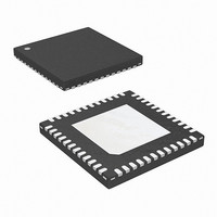
ISL6262CRZ-T Intersil, ISL6262CRZ-T Datasheet - Page 24

ISL6262CRZ-T
Manufacturer Part Number
ISL6262CRZ-T
Description
IC CORE REG 2PHASE 48-QFN
Manufacturer
Intersil
Datasheet
1.ISL6262CRZ.pdf
(27 pages)
Specifications of ISL6262CRZ-T
Applications
Converter, Intel IMVP-6
Voltage - Input
5 ~ 25 V
Number Of Outputs
1
Voltage - Output
0.3 ~ 1.5 V
Operating Temperature
-10°C ~ 100°C
Mounting Type
Surface Mount
Package / Case
48-VQFN
Lead Free Status / RoHS Status
Lead free / RoHS Compliant
Available stocks
Company
Part Number
Manufacturer
Quantity
Price
Dynamic Mode of Operation - Dynamic Droop
Using DCR Sensing
Droop is very important for load transient performance. If the
system is not compensated correctly, the output voltage
could sag excessively upon load application and potentially
create a system failure. The output voltage could also take a
long period of time to settle to its final value. This could be
problematic if a load dump were to occur during this time.
This situation would cause the output voltage to rise above
the no load setpoint of the converter and could potentially
damage the CPU.
The L/DCR time constant of the inductor must be matched to
the Rn*Cn time constant as shown in the following equation:
Solving for Cn we now have the following equation:
Note, RO was neglected. As long as the inductor time
constant matches the Cn, Rn and Rs time constants as
given above, the transient performance will be optimum. As
in the static droop case, this process may require a slight
adjustment to correct for layout inconsistencies. For the
example of L = 0.36µH with 0.8mΩ DCR, Cn is calculated
below.
The value of this capacitor is selected to be 330nF. As the
inductors tend to have 20% to 30% tolerances, this cap
generally will be tuned on the board by examining the
transient voltage. If the output voltage transient has an initial
dip, lower than the voltage required by the load line, and
slowly increases back to the steady state, the cap is too
small and vice versa. It is better to have the cap value a little
C
C
-------------
DCR
FIGURE 35. LOAD LINE PERFORMANCE WITH NTC
n
n
L
2.25
2.15
2.05
=
=
2.2
2.1
---------------------------------- -
----------------------------------
R
------------------------------------------------------------------
parallel 5.87K, 1.825K
R
=
0
n
n
R
--------------------------------- - C
R
+
•
-------------
DCR
n
n
RS
RS
L
+
•
RS
RS
EQV
THERMAL COMPENSATION
EQV
0.36μH
------------------- -
(
0.0008
EQV
EQV
20
INDUCTOR TEMPERATURE (°C)
•
n
40
)
24
≈
330nF
60
80
(EQ. 24)
(EQ. 25)
(EQ. 23)
100
ISL6262
bigger to cover the tolerance of the inductor to prevent the
output voltage from going lower than the spec. This cap
needs to be a high grade cap like X7R with low tolerance.
There is another consideration in order to achieve better
time constant match mentioned above. The NPO/COG
(class-I) capacitors have only 5% tolerance and a very good
thermal characteristics. But those caps are only available in
small capacitance values. In order to use such capacitors,
the resistors and thermistors surrounding the droop voltage
sensing and droop amplifier has to be resized up to 10X to
reduce the capacitance by 10X. But attention has to be paid
in balancing the impedance of droop amplifier in this case.
Dynamic Mode of Operation - Compensation
Parameters
Considering the voltage regulator as a black box with a
voltage source controlled by VID and a series impedance, in
order to achieve the 2.1mV/A load line, the impedance
needs to be 2.1mΩ. The compensation design has to target
the output impedance of the converter to be 2.1mΩ. There is
a mathematical calculation file available to the user. The
power stage parameters such as L and Cs are needed as
the input to calculate the compensation component values.
Attention has to be paid to the input resistor to the FB pin.
Too high of a resistor will cause an error to the output voltage
regulation because of bias current flowing in the FB pin. It is
better to keep this resistor below 3K when using this file.
Static Mode of Operation - Current Balance Using
DCR or Discrete Resistor Current Sensing
Current Balance is achieved in the ISL6262 through the
matching of the voltages present on the ISEN pins. The
ISL6262 adjusts the duty cycles of each phase to maintain
equal potentials on the ISEN pins. RL and CL around each
inductor, or around each discrete current resistor, are used
to create a rather large time constant such that the ISEN
voltages have minimal ripple voltage and represent the DC
current flowing through each channel's inductor. For
optimum performance, RL is chosen to be 10kΩ and CL is
selected to be 0.22µF. When discrete resistor sensing is
used, a capacitor most likely needs to be placed in parallel
with RL to properly compensate the current balance circuit.
ISL6262 uses RC filter to sense the average voltage on
phase node and forces the average voltage on the phase
node to be equal for current balance. Even though the
ISL6262 forces the ISEN voltages to be almost equal, the
inductor currents will not be exactly equal. Take DCR current
sensing as example, two errors have to be added to find the
total current imbalance. 1) Mismatch of DCR: If the DCR has
a 5% tolerance then the resistors could mismatch by 10%
worst case. If each phase is carrying 20A then the phase
currents mismatch by 20A*10% = 2A. 2) Mismatch of phase
voltages/offset voltage of ISEN pins. The phase voltages are
within 2mV of each other by current balance circuit. The
error current that results is given by 2mV/DCR. If
DCR = 1mΩ then the error is 2A.
May 15, 2006
FN9199.2


