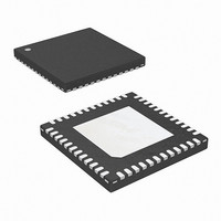
ISL6333BIRZ Intersil, ISL6333BIRZ Datasheet - Page 25

ISL6333BIRZ
Manufacturer Part Number
ISL6333BIRZ
Description
IC CTRLR PWM 3PHASE BUCK 48-QFN
Manufacturer
Intersil
Datasheet
1.ISL6333ACRZ.pdf
(40 pages)
Specifications of ISL6333BIRZ
Applications
Controller, Intel VR11
Voltage - Input
5 ~ 12 V
Number Of Outputs
1
Voltage - Output
0.5 ~ 1.6 V
Operating Temperature
-40°C ~ 85°C
Mounting Type
Surface Mount
Package / Case
48-VQFN
Lead Free Status / RoHS Status
Lead free / RoHS Compliant
In Equation 10, V
programmed offset voltage, I
the converter, R
to the ISEN+ pin, R
number of channels, and DCR is the Inductor DCR value.
Therefore the equivalent loadline impedance, i.e. droop
impedance, is equal to Equation 11:
Output-Voltage Offset Programming
The controllers allow the designer to accurately adjust the
offset voltage by connecting a resistor, R
pin to VCC or GND. When R
and VCC, the voltage across it is regulated to 1.6V. This
causes a proportional current (I
and out of the FB pin, providing a negative offset. If R
connected to ground, the voltage across it is regulated to
0.3V, and I
providing a positive offset. The offset current flowing through
the resistor between VSEN and FB will generate the desired
offset voltage which is equal to the product (I
These functions are shown in Figures 8 and 9.
Once the desired output offset voltage has been determined,
use Equations 12 and 13 to set R
For Negative Offset (connect R
For Positive Offset (connect R
R
R
R
V
R
OFS
OFS
LL
OFS
OFS
FIGURE 8. POSITIVE OFFSET OUTPUT VOLTAGE
+
-
VDIFF
=
=
=
------------
R
GND
R
I
N
--------------------------
V
--------------------------
V
OFS
FB
1.6 R
0.3 R
FB
OFS
OFFSET
OFFSET
OFS
FB
⋅
⋅
⋅
-------------- -
R
DCR
PROGRAMMING
SET
FB
FB
flows into the FB pin and out of the OFS pin,
ISEN
REF
FB
⋅
ISL6333 INTERNAL CIRCUIT
400
--------- -
is the internal sense resistor connected
3
is the reference voltage, V
is the feedback resistor, N is the active
VREF
OUT
OFS
25
OFS
OFS
OFS
is the total output current of
is connected between OFS
OFS
to GND):
) to flow into the OFS pin
to VCC):
ISL6333, ISL6333A, ISL6333B, ISL6333C
:
OFS
E/A
GND
+
-
OFS
, from the OFS
0.3V
OFS
x R
VCC
is the
(EQ. 11)
FB
(EQ. 12)
(EQ. 13)
OFS
+
-
1.6V
).
is
Dynamic VID
Modern microprocessors need to make changes to their core
voltage as part of normal operation. They direct the controllers
to do this by making changes to the VID inputs. The
controllers are required to monitor the DAC inputs and
respond to on-the-fly VID changes in a controlled manner,
supervising a safe output voltage transition without
discontinuity or disruption.
The controllers check for VID changes by comparing the
internal DAC code to the VID pin inputs on the positive edge
of an internal 5.55MHz clock. If a new code is established on
the VID inputs and it remains stable for 3 consecutive
readings (360ns to 540ns), the controllers recognize the new
code and begins incrementing/decrementing the DAC in
6.25mV steps at a stepping frequency of 1.85MHz. This
controlled slew rate of 6.25mV/540ns (11.6mV/µs) continues
until the VID input and DAC are equal. Thus, the total time
required for a VID change, t
of the VID change (ΔV
The time required for a ISL6333-based converter to make a
1.6V to 0.5V reference voltage change is about 95µs, as
calculated using Equation 14.
VID “Off” DAC Codes
The Intel VR11 VID tables include “Off” DAC codes, which
indicate to the controllers to disable all regulation. Recognition
of these codes is slightly different in that they must be stable for
4 consecutive readings of a 5.55MHz clock (540ns to 720ns)
to be recognized. Once an “Off” code is recognized the
controllers latch off, and must be reset by toggling the EN pin.
t
DVID
V
R
OFS
OFS
FIGURE 9. NEGATIVE OFFSET OUTPUT VOLTAGE
+
-
VDIFF
VCC
=
I
OFS
R
540 10
FB
OFS
FB
⋅
PROGRAMMING
–
9
⋅
⎛
⎝
ISL6333 INTERNAL CIRCUIT
-------------------- -
0.00625
Δ
VID
V
VREF
VID
).
DVID
⎞
⎠
, is dependent only on the size
E/A
GND
+
-
0.3V
October 8, 2010
VCC
(EQ. 14)
FN6520.3
+
-
1.6V


