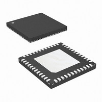
ISL6312CRZ-TK Intersil, ISL6312CRZ-TK Datasheet - Page 24

ISL6312CRZ-TK
Manufacturer Part Number
ISL6312CRZ-TK
Description
IC CTRLR PWM 4PHASE BUCK 48-QFN
Manufacturer
Intersil
Datasheet
1.ISL6312CRZ.pdf
(35 pages)
Specifications of ISL6312CRZ-TK
Applications
Controller, Intel VR10, VR11, AMD CPU
Voltage - Input
5 ~ 12 V
Number Of Outputs
1
Voltage - Output
0.38 ~ 1.6 V
Operating Temperature
0°C ~ 70°C
Mounting Type
Surface Mount
Package / Case
48-VQFN
Lead Free Status / RoHS Status
Lead free / RoHS Compliant
Fault Monitoring and Protection
The ISL6312 actively monitors output voltage and current to
detect fault conditions. Fault monitors trigger protective
measures to prevent damage to a microprocessor load. One
common power good indicator is provided for linking to
external system monitors. The schematic in Figure 14
outlines the interaction between the fault monitors and the
power good signal.
Power Good Signal
The power good pin (PGOOD) is an open-drain logic output
that signals whether or not the ISL6312 is regulating the
output voltage within the proper levels, and whether any fault
conditions exist. This pin should be tied to a +5V source
through a resistor.
During shutdown and soft-start PGOOD pulls low and
releases high after a successful soft-start and the output
voltage is operating between the undervoltage and
overvoltage limits. PGOOD transitions low when an
undervoltage, overvoltage, or overcurrent condition is
detected or when the controller is disabled by a reset from
EN, EN_PH4, POR, or one of the no-CPU VID codes. In the
event of an overvoltage or overcurrent condition, the
controller latches off and PGOOD will not return high until
after a successful soft-start. In the case of an undervoltage
event, PGOOD will return high when the output voltage
returns to within the undervoltage.
FIGURE 14. POWER GOOD AND PROTECTION CIRCUITRY
VRSEL
OVPSEL
VSEN
RGND
VDIFF
+
-
V
OVP
x1
+250mV,
+175mV,
+350mV
VDAC
0.60 x DAC
+
+
-
-
AND CONTROL LOGIC
24
UV
OV
SOFT-START, FAULT
ISL6312 INTERNAL CIRCUITRY
EACH CHANNEL
OCL
REPEAT FOR
OCP
+
-
+
-
170µA
I
1
125µA
I
AVG
PGOOD
ISL6312
Overvoltage Protection
The ISL6312 constantly monitors the sensed output voltage
on the VDIFF pin to detect if an overvoltage event occurs.
When the output voltage rises above the OVP trip level
actions are taken by the ISL6312 to protect the
microprocessor load. The overvoltage protection trip level
changes depending on what mode of operation the controller
is in and what state the OVPSEL and VRSEL pins are in.
Tables 6 and 7 list what the OVP trip levels are under all
conditions.
At the inception of an overvoltage event, LGATE1, LGATE2
and LGATE3 are commanded high, PWM4 is commanded
low, and the PGOOD signal is driven low. This turns on the
all of the lower MOSFETs and pulls the output voltage below
a level that might cause damage to the load. The LGATE
outputs remain high and PWM4 remains low until VDIFF falls
100mV below the OVP threshold that tripped the overvoltage
protection circuitry. The ISL6312 will continue to protect the
load in this fashion as long as the overvoltage condition
recurs. Once an overvoltage condition ends the ISL6312
latches off, and must be reset by toggling EN, or through
POR, before a soft-start can be reinitiated.
One exception that overrides the overvoltage protection
circuitry is a dynamic VID transition in AMD modes of
operation. If a new VID code is detected during normal
operation, the OVP protection circuitry is disabled from the
beginning of the dynamic VID transition, until 50µs after the
internal DAC reaches the final VID setting. This is the only
time during operation of the ISL6312 that the OVP circuitry is
not active.
Pre-POR Overvoltage Protection
Prior to PVCC and VCC exceeding their POR levels, the
ISL6312 is designed to protect the load from any overvoltage
events that may occur. This is accomplished by means of an
internal 10kΩ resistor tied from PHASE to LGATE, which
Soft-Start
(TD1 and TD2)
Soft-Start
(TD3 and TD4)
Normal Operation
Soft-Start
Normal Operation
OPERATION
OPERATION
TABLE 6. INTEL VR10 AND VR11 OVP THRESHOLDS
MODE OF
MODE OF
TABLE 7. AMD OVP THRESHOLDS
OVPSEL PIN OPEN
OVPSEL PIN OPEN
OR TIED TO GND
OR TIED TO GND
(higher of the two)
(higher of the two)
VDAC + 175mV
VDAC + 175mV
VDAC + 175mV
VDAC + 250mV
VDAC + 250mV
1.280V and
2.200V and
OVPSEL PIN TIED
OVPSEL PIN TIED
(higher of the two)
(higher of the two)
VDAC + 350mV
VDAC + 350mV
VDAC + 350mV
VDAC + 350mV
VDAC + 350mV
1.280V and
2.200V and
TO VCC
TO VCC
February 1, 2011
FN9289.6


