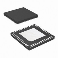
ISL6312CRZ-TK Intersil, ISL6312CRZ-TK Datasheet - Page 9

ISL6312CRZ-TK
Manufacturer Part Number
ISL6312CRZ-TK
Description
IC CTRLR PWM 4PHASE BUCK 48-QFN
Manufacturer
Intersil
Datasheet
1.ISL6312CRZ.pdf
(35 pages)
Specifications of ISL6312CRZ-TK
Applications
Controller, Intel VR10, VR11, AMD CPU
Voltage - Input
5 ~ 12 V
Number Of Outputs
1
Voltage - Output
0.38 ~ 1.6 V
Operating Temperature
0°C ~ 70°C
Mounting Type
Surface Mount
Package / Case
48-VQFN
Lead Free Status / RoHS Status
Lead free / RoHS Compliant
Functional Pin Descriptions
VCC
VCC is the bias supply for the ICs small-signal circuitry.
Connect this pin to a +5V supply and decouple using a
quality 0.1µF ceramic capacitor.
PVCC1_2 and PVCC3
These pins are the power supply pins for the corresponding
channel MOSFET drive, and can be connected to any
voltage from +5V to +12V depending on the desired
MOSFET gate-drive level. Decouple these pins with a quality
1.0µF ceramic capacitor.
Leaving PVCC3 unconnected or grounded programs the
controller for 2-phase operation.
GND
GND is the bias and reference ground for the IC.
EN
This pin is a threshold-sensitive (approximately 0.85V) enable
input for the controller. Held low, this pin disables controller
operation. Pulled high, the pin enables the controller for
operation.
FS
A resistor, placed from FS to ground, sets the switching
frequency of the controller.
VID0, VID1, VID2, VID3, VID4, VID5, VID6, and VID7
These are the inputs for the internal DAC that provides the
reference voltage for output regulation. These pins respond to
TTL logic thresholds. These pins are internally pulled high, to
approximately 1.2V, by 40µA internal current sources for Intel
modes of operation, and pulled low by 20µA internal current
sources for AMD modes of operation. The internal pull-up
current decreases to 0 as the VID voltage approaches the
internal pull-up voltage. All VID pins are compatible with
external pull-up voltages not exceeding the IC’s bias voltage
(VCC).
VRSEL
The state of this pin selects which of the available DAC tables
will be used to decode the VID inputs and puts the controller
into the corresponding mode of operation. Refer to Table 1 for
available options and details of implementation.
VSEN and RGND
VSEN and RGND are inputs to the precision differential
remote-sense amplifier and should be connected to the sense
pins of the remote load.
VDIFF
VDIFF is the output of the differential remote-sense amplifier.
The voltage on this pin is equal to the difference between
VSEN and RGND.
9
ISL6312
ISL6312
FB and COMP
These pins are the internal error amplifier inverting input and
output respectively. FB, VDIFF, and COMP are tied together
through external R-C networks to compensate the regulator.
IDROOP
The IDROOP pin is the average channel-current sense
output. Connecting this pin through a tuned parallel R-C
network to FB allows the converter to incorporate output
voltage droop proportional to the output current. If voltage
droop is not desired leave this pin unconnected.
REF
The REF input pin is the positive input of the error amplifier. It
is internally connected to the DAC output through a 1kΩ
resistor. A capacitor is used between the REF pin and ground
to smooth the voltage transition during Dynamic VID
operations.
OFS
The OFS pin provides a means to program a DC current for
generating an offset voltage across the resistor between FB
and VDIFF. The offset current is generated via an external
resistor and precision internal voltage references. The polarity
of the offset is selected by connecting the resistor to GND or
VCC. For no offset, the OFS pin should be left unconnected.
ISEN1-, ISEN1+, ISEN2-, ISEN2+, ISEN3-, ISEN3+,
ISEN4-, and ISEN4+
These pins are used for differentially sensing the
corresponding channel output currents. The sensed currents
are used for channel balancing, protection, and load line
regulation.
Connect ISEN1-, ISEN2-, ISEN3-, and ISEN4- to the node
between the RC sense elements surrounding the inductor of
their respective channel. Tie the ISEN+ pins to the VCORE
side of their corresponding channel’s sense capacitor.
UGATE1, UGATE2, and UGATE3
Connect these pins to the corresponding upper MOSFET
gates. These pins are used to control the upper MOSFETs
and are monitored for shoot-through prevention purposes.
BOOT1, BOOT2, and BOOT3
These pins provide the bias voltage for the corresponding
upper MOSFET drives. Connect these pins to appropriately-
chosen external bootstrap capacitors. Internal bootstrap
diodes connected to the PVCC pins provide the necessary
bootstrap charge.
February 1, 2011
FN9289.6


