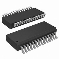
ISL6539CA-T Intersil, ISL6539CA-T Datasheet - Page 11

ISL6539CA-T
Manufacturer Part Number
ISL6539CA-T
Description
IC CTRLR DDR DRAM, SDRAM 28QSOP
Manufacturer
Intersil
Datasheet
1.ISL6539CAZ.pdf
(20 pages)
Specifications of ISL6539CA-T
Applications
Controller, DDR DRAM, SDRAM
Voltage - Input
3.3 ~ 18 V
Number Of Outputs
2
Voltage - Output
0.9 ~ 5.5 V
Operating Temperature
0°C ~ 70°C
Mounting Type
Surface Mount
Package / Case
28-QSOP
Lead Free Status / RoHS Status
Contains lead / RoHS non-compliant
The small signal transfer function from the error amplifier
output voltage V
Equation 7:
The DC gain is derived by shorting the inductor and opening
the capacitor. There is one zero and two poles in this transfer
function.
The zero is related to ESR and the output capacitor.
The first pole is a low frequency pole associated with the
output capacitor and its charging resistors. The inductor can
be regarded as short. The second pole is the high frequency
pole related to the inductor. At high frequency the output cap
can be regarded as a short circuit. By approximation, the
poles and zero are inversely proportional to the time
constants, associated with inductor and capacitor, by
Equations 8, 9 and 10:
Wz
Wp1
Wp2
Since the current loop separates the LC resonant poles into
two distant poles, and ESR zero tends to cancel the high
frequency pole, the second order system behaves like a first
order system. This control method simplifies the design of
the internal compensator and makes it possible to
Ch1 and Ch2 Input Voltage Input voltage > 4.2V
Ch1
Ch2
G s ( )
TABLE 1. PWM COMPARATOR RAMP AMPLITUDE FOR
TABLE 2. PWM COMPARATOR RAMP VOLTAGE AMPLITUDE
=
=
=
=
----------------------- -
ESR*C
------------------------------------------------------------------------------ -
(
R
--------------------------------------------------------- -
G
Input Voltage
GND
Input voltage >4.2V
GND
ESR
i
m
1
+
DCR
---------------------------------------
R
DUAL SWITCHER APPLICATION
FOR DDR APPLICATION
o
+
i
GND
+
(
VIN PIN CONNECTION
R
c
DCR
L
+
i
o
R
to the output voltage V
+
VIN PIN CONNECTIONS
ESR
o
DCR
1
+
R
||
o
) R
R
Input voltage > 4.2V
Input voltage < 4.2V
||
o
---------------------------------------------------------
⎛
⎝
Input voltage < 4.2V
------------ -
Wp1
o
11
s
)*C
⎛
⎝
+
o
-------- -
Wz
s
1
⎞
⎠
⎛
⎝
+
------------ -
Wp2
1
s
⎞
⎠
o
can be written in
+
1
⎞
⎠
AMPLITUDE
AMPLITUDE
VRAMP
VRAMP
0.625V
1.25V
1.25V
1.25V
V
1.25V
1.25V
V
IN
IN
(EQ. 10)
/8
(EQ. 7)
(EQ. 9)
/8
(EQ. 8)
ISL6539
accommodate many applications having a wide range of
parameters. The schematic for the internal compensator is
shown in Figure 8.
Its transfer function can be written as Equation 11:
where:
f
Outside the ISL6539 chip, a capacitor C
parallel with the top resistor in the feedback resistor divider,
as shown in Figure 6. In this case the transfer function from
the output voltage to the middle point of the divider can be
written as:
The ratio of R
set point; therefore, the position of the pole and zero
frequency in Equation 12 may not be far apart; however,
they can improve the loop gain and phase margin with the
proper design.
The C
variation directly to the VSEN pin to cause the PGOOD drop.
Such an effect should be considered in the selection of C
From the analysis in Equation 12, the system loop gain can
be written as Equation 13:
Figure 9 shows the composition of the system loop gain. As
shown in the graph, the power stage became a well damped
second order system compared to the LC filter
characteristics. The ESR zero is so close to the high
frequency pole that they cancel each other out. The power
stage behaves like a first order system. With an internal
compensator, the loop gain transfer function has a cross
over frequency at about 30kHz. With a given set of
parameters, including the MOSFET r
Gloop s ( )
Gcomp s ( )
Gfd s ( )
z1
= 6.98kHz, f
z
TO PWM
COMPARATOR
=
can bring the high frequency transient output voltage
FIGURE 8. THE INTERNAL COMPENSATOR
=
-------------------- -
R
=
1
G s ( ) Gcomp s ( )
R
+
1.857 10
-------------------------------------------------------------------------------------------- -
2
1
ISEN
4.4k
R
and R
z2
2
•
--------------------------------------------- -
s R
= 380kHz, and f
(
•
sR
1
2
||
5
1
s
is determined by the output voltage
1.25pF
1M 16.7pF
R
⎛
⎝
C
⎛
⎝
-------------- -
2πf
2
-------------- -
2πf
z
Vc
)C
s
+
s
z1
•
p1
1
z
Gfd
+
+
+
-
+
1
1
1
⎞
⎠
s ( )
500k
⎞
⎠
⎛
⎝
p1
0.9V
-------------- -
2πf
DS(ON)
s
= 137kHz
z2
300k
z
+
can be placed in
1
⎞
⎠
, current sense
VSEN
April 29, 2010
(EQ. 11)
(EQ. 12)
(EQ. 13)
FN9144.6
z
.


