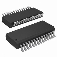
ISL6539CA-T Intersil, ISL6539CA-T Datasheet - Page 13

ISL6539CA-T
Manufacturer Part Number
ISL6539CA-T
Description
IC CTRLR DDR DRAM, SDRAM 28QSOP
Manufacturer
Intersil
Datasheet
1.ISL6539CAZ.pdf
(20 pages)
Specifications of ISL6539CA-T
Applications
Controller, DDR DRAM, SDRAM
Voltage - Input
3.3 ~ 18 V
Number Of Outputs
2
Voltage - Output
0.9 ~ 5.5 V
Operating Temperature
0°C ~ 70°C
Mounting Type
Surface Mount
Package / Case
28-QSOP
Lead Free Status / RoHS Status
Contains lead / RoHS non-compliant
Due to the nature of the current sensing technique and to
accommodate a wide range of the r
value of the overcurrent threshold should set at about 180%
of the nominal load value. If more accurate current
protection is desired, a current sense resistor placed in
series with the lower MOSFET source may be used. The
inductor current going through the lower MOSFET is sensed
and held at 400ns after the upper MOSFET is turned off;
therefore, the sensed current is very close to its peak value.
The inductor peak current can be written as Equation 15:
As seen from Equation 15, the inductor peak current
changes with the input voltage and the inductor value once
an output voltage is selected.
After overcurrent protection is activated, there are two ways
to bring the offending channel back: (1) Both EN1 and EN2
have to be held low to clear the latch, (2) To recycle the V
of the chip, the POR will clear the latch.
Undervoltage Protection
In the process of operation, if a short circuit occurs, the
output voltage will drop quickly. Before the overcurrent
protection circuit responds, the output voltage will fall out of
the required regulation range. The chip comes with
undervoltage protection. If a load step is strong enough to
pull the output voltage lower than the undervoltage
threshold, the offending channel latches off immediately. The
undervoltage threshold is 75% of the nominal output voltage.
Toggling both enables to low, or recycling V
latch and bring the chip back to operation.
Overvoltage Protection
Should the output voltage increase over 115% of the normal
value due to the upper MOSFET failure, or for other reasons,
the overvoltage protection comparator will force the
synchronous rectifier gate driver high. This action actively
pulls down the output voltage. As soon as the output voltage
drops below the threshold, the OVP comparator is
disengaged. The MOSFET driver will restore its normal
operation. When the OVP occurs, the PGOOD will drop to
low as well.
I
peak
=
3
1
2
(
-------------------------------------------------- -
FIGURE 10. OVERCURRENT PROTECTION
V
Ch1 5.0V
Ch3 1.0A Ω
2L f
IN
IL
–
•
V
SW
out
) V
•
PGOOD
•
VOUT
V
IN
out
Ch2 100mV
+
I
load
13
8 CLK
DS(ON)
SHUTDOWN
CC
variation, the
M 10.0 μs
, will clear the
(EQ. 15)
CC
ISL6539
This OVP scheme provides a ‘soft’ crowbar function, which
helps clamp the voltage overshoot, and does not invert the
output voltage when otherwise activated with a continuously
high output from lower MOSFET driver (a common problem
for OVP schemes with a latch).
DDR Application
High throughput Double Data Rate (DDR) memory chips are
expected to take the place of traditional memory chips. A
novel feature associated with this type of memory are the
referencing and data bus termination techniques. These
techniques employ a reference voltage, VREF, that tracks
the center point of VDDQ and VSS voltages, and an
additional VTT power source where all terminating resistors
are connected. Despite the additional power source, the
overall memory power consumption is reduced compared to
traditional termination.
The added power source has a cluster of requirements that
should be observed and considered. Due to the reduced
differential thresholds of DDR memory, the termination
power supply voltage, VTT, closely tracks VDDQ/2 voltage.
Another very important feature of the termination power
supply is the capability to operate at equal efficiency in
sourcing and sinking modes. The VTT supply regulates the
output voltage with the same degree of precision when
current is flowing from the supply to the load, and when the
current is diverted back from the load into the power supply.
The ISL6539 dual channel PWM controller possesses
several important enhancements that allow re-configuration
for DDR memory applications, and provides all three
voltages required in a DDR memory compliant computer.
To reconfigure the ISL6539 for a complete DDR solution, the
DDR pin should be set high permanently to the VCC rail.
This activates some functions inside the chip that are
specific to DDR memory power needs.
In the DDR application presented in Figure 4, the first
controller regulates the VDDQ rail to 2.5V. The output
voltage is set by external dividers Rfb1 and Rfb12. The
second controller regulates the VTT rail to VDDQ/2. The
OCSET2 pin function is now different, and serves as an
input that brings VDDQ/2 voltage, created by the Rd1 and
Rd2 divider, inside the chip, effectively providing a tracking
function for the VTT voltage.
The PG2 pin function is also different in DDR mode. This pin
becomes the output of the buffer, whose input is connected
to the center point of the R/R divider from the VDDQ output
by the OCSET2 pin. The buffer output voltage serves as a
1.25V reference for the DDR memory chips. Current
capability of this pin is 10mA (12mA max).
For the VTT channel where output is derived from the VDDQ
output, some control and protective functions have been
significantly simplified. For example, the overcurrent, and
overvoltage, and undervoltage protections for the second
April 29, 2010
FN9144.6


