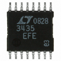
LT3435EFE#PBF Linear Technology, LT3435EFE#PBF Datasheet - Page 16

LT3435EFE#PBF
Manufacturer Part Number
LT3435EFE#PBF
Description
IC REG SW HV 3A 500KHZ 16-TSSOP
Manufacturer
Linear Technology
Type
Step-Down (Buck)r
Datasheet
1.LT3435EFEPBF.pdf
(24 pages)
Specifications of LT3435EFE#PBF
Internal Switch(s)
Yes
Synchronous Rectifier
No
Number Of Outputs
1
Voltage - Output
1.25 ~ 54 V
Current - Output
3A
Frequency - Switching
500kHz
Voltage - Input
3.3 ~ 60 V
Operating Temperature
-40°C ~ 125°C
Mounting Type
Surface Mount
Package / Case
16-TSSOP Exposed Pad, 16-eTSSOP, 16-HTSSOP
Primary Input Voltage
60V
No. Of Outputs
1
Output Voltage
68V
Output Current
2.4A
No. Of Pins
16
Operating Temperature Range
-40°C To +125°C
Msl
MSL 1 - Unlimited
Rohs Compliant
Yes
Lead Free Status / RoHS Status
Lead free / RoHS Compliant
Power - Output
-
Available stocks
Company
Part Number
Manufacturer
Quantity
Price
LT3435
APPLICATIO S I FOR ATIO
If a no load condition can be anticipated, the supply current
can be further reduced by cycling the SHDN pin at a rate
higher than the natural no load burst frequency. Figure 6
shows Burst Mode operation with the SHDN pin. V
burst ripple is maintained while the average supply current
drops to 15µA. The PG pin will be active low during the
“on” portion of the SHDN waveform due to the C
tor discharge when SHDN is taken low. See the Power
Good section for further information.
CATCH DIODE
The catch diode carries load current during the SW off
time. The average diode current is therefore dependent on
the switch duty cycle. At high input to output voltage ratios
the diode conducts most of the time. As the ratio ap-
proaches unity the diode conducts only a small fraction of
the time. The most stressful condition for the diode is
when the output is short circuited. Under this condition the
diode must safely handle I
To maximize high and low load current efficiency a fast
switching diode with low forward drop and low reverse
leakage should be used. Low reverse leakage is critical to
maximize low current efficiency since its value over tem-
perature can potentially exceed the magnitude of the
LT3435 supply current. Low forward drop is critical for
high current efficiency since the loss is proportional to
forward drop.
These requirements result in the use of a Schottky type
diode. DC switching losses are minimized due to its low
forward voltage drop and AC behavior is benign due to its
16
AC-COUPLED
50mV/DIV
2V/DIV
1A/DIV
V
V
SHDN
OUT
I
SW
Figure 6. Burst Mode with Shutdown Pin
V
V
I
Q
IN
OUT
= 15µA
= 12V
= 3.3V
U
100ms/DIV
U
PEAK
at maximum duty cycle.
W
3435 F06
U
T
capaci-
OUT
Table 4. Catch Diode Selection Criteria
DIODE
IR 10BQ100 0.0µA
Diodes Inc.
B260SMA
Diodes Inc.
B360SMB
IR
MBRS360TR
IR 30BQ100 1.7µA 2.64mA 0.40V
lack of a significant reverse recovery time. Schottky diodes
are generally available with reverse voltage ratings of 60V
and even 100V and are price competitive with other types.
The effect of reverse leakage and forward drop on effi-
ciency for various Schottky diodes is shown in Table 4. As
can be seen these are conflicting parameters and the user
must weigh the importance of each specification in choos-
ing the best diode for the application.
The use of so-called “ultrafast” recovery diodes is gener-
ally not recommended. When operating in continuous
mode, the reverse recovery time exhibited by “ultrafast”
diodes will result in a slingshot type effect. The power
internal switch will ramp up V
attempt to get it to recover. Then, when the diode has
finally turned off, some tens of nanoseconds later, the V
node voltage ramps up at an extremely high dV/dt, per-
haps 5V to even 10V/ns! With real world lead inductances
the V
result in poor RFI behavior and, if the overshoot is severe
enough, damage the IC itself.
BOOST PIN
For most applications the boost components are a 0.33µF
capacitor and a MMSD914 diode. The anode is typically
connected to the regulated output voltage to generate a
voltage approximately V
stage (Figure 7a). However, the output stage discharges
the boost capacitor during the on time of the switch. The
output driver requires at least 2.5V of headroom through-
out this period to keep the switch fully saturated. If the
SW
node can easily overshoot the V
0.1µA
0.2µA
25°C
1µA
V
LEAKAGE
OUT
= 3.3V
1.81mA 0.42V
242µA 0.48V
440µA 0.45V
125°C
59µA
OUT
0.72V
25°C
V
F
above V
IN
AT 1A
current into the diode in an
125°C
0.58V
0.41V
0.36V
0.34V
0.32V
IN
I
V
Q
V
to drive the output
OUT
1088µA
at 125°C EFFICIENCY
IN
I
125µA
215µA
270µA
821µA
L
=12V
= 0A
IN
= 3.3 V
rail. This can
OUT
V
I
74.7%
81.7%
82.4%
82.7%
81.1%
L
IN
= 1A
=12V
= 3.3V
3435fa
SW


