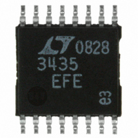
LT3435EFE#PBF Linear Technology, LT3435EFE#PBF Datasheet - Page 9

LT3435EFE#PBF
Manufacturer Part Number
LT3435EFE#PBF
Description
IC REG SW HV 3A 500KHZ 16-TSSOP
Manufacturer
Linear Technology
Type
Step-Down (Buck)r
Datasheet
1.LT3435EFEPBF.pdf
(24 pages)
Specifications of LT3435EFE#PBF
Internal Switch(s)
Yes
Synchronous Rectifier
No
Number Of Outputs
1
Voltage - Output
1.25 ~ 54 V
Current - Output
3A
Frequency - Switching
500kHz
Voltage - Input
3.3 ~ 60 V
Operating Temperature
-40°C ~ 125°C
Mounting Type
Surface Mount
Package / Case
16-TSSOP Exposed Pad, 16-eTSSOP, 16-HTSSOP
Primary Input Voltage
60V
No. Of Outputs
1
Output Voltage
68V
Output Current
2.4A
No. Of Pins
16
Operating Temperature Range
-40°C To +125°C
Msl
MSL 1 - Unlimited
Rohs Compliant
Yes
Lead Free Status / RoHS Status
Lead free / RoHS Compliant
Power - Output
-
Available stocks
Company
Part Number
Manufacturer
Quantity
Price
BLOCK DIAGRA
APPLICATIO S I FOR ATIO
power from the V
an external voltage higher than 3V bias power will be
drawn from the external source (typically the regulated
output voltage). This improves efficiency.
High switch efficiency is attained by using the BOOST pin
to provide a voltage to the switch driver which is higher
than the input voltage, allowing switch to be saturated.
This boosted voltage is generated with an external capaci-
tor and diode.
FEEDBACK PIN FUNCTIONS
The feedback (FB) pin on the LT3435 is used to set output
voltage and provide several overload protection features.
The first part of this section deals with selecting resistors
to set output voltage and the remaining part talks about
frequency foldback and soft-start features. Please read
both parts before committing to a final design.
Referring to Figure 2, the output voltage is determined by
a voltage divider from V
1.25V at the FB pin. Since the output divider is a load on the
output care must be taken when choosing the resistor
divider values. For light load applications the resistor
values should be as large as possible to achieve peak
efficiency in Burst Mode operation. Extremely large values
for resistor R1 will cause an output voltage error due to the
50nA FB pin input current. The suggested value for the
output divider resistor (see Figure 2) from FB to ground
(R2) is 100k or less. A formula for R1 is shown below. A
table of standard 1% values is shown in Table 1 for
common output voltages.
More Than Just Voltage Feedback
The FB pin is used for more than just output voltage
sensing. It also reduces switching frequency and con-
trols the soft-start voltage ramp rate when output voltage
is below the regulated level (see the Frequency Foldback
R
1
=
R
2
•
1 25
.
V
OUT
IN
+
U
pin, but if the BIAS pin is connected to
R
– .
2 50
1 25
•
OUT
U
W
nA
to ground which generates
W
U
To further optimize efficiency, the LT3435 automatically
switches to Burst Mode operation in light load situations.
In Burst Mode operation, all circuitry associated with
controlling the output switch is shut down reducing the
input supply current to 45µA.
The LT3435 contains a power good flag with a program-
mable threshold and delay time. A logic-level low on the
SHDN pin disables the IC and reduces input suppy current
to less than 1µA.
Table 1
LT3435
OSCILLATOR
VOLTAGE
OUTPUT
500kHz
(V)
2.5
3.3
10
12
3
5
6
8
Figure 2. Feedback Network
(kΩ, 1%)
100
100
100
100
100
100
100
100
R2
SOFT-START
FOLDBACK
DETECT
ERROR
AMP
NEAREST (1%)
–
+
(kΩ)
100
140
165
301
383
536
698
866
R1
1.25V
C
SW
SS
FB
V
C
12
11
LT3435
2
9
3435 F02
C1
OUTPUT
ERROR
– 0.63
– 0.25
0.38
0.25
0.63
0.63
(%)
0
0
R1
R2
3435fa
V
9
OUT


