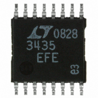
LT3435EFE#PBF Linear Technology, LT3435EFE#PBF Datasheet - Page 17

LT3435EFE#PBF
Manufacturer Part Number
LT3435EFE#PBF
Description
IC REG SW HV 3A 500KHZ 16-TSSOP
Manufacturer
Linear Technology
Type
Step-Down (Buck)r
Datasheet
1.LT3435EFEPBF.pdf
(24 pages)
Specifications of LT3435EFE#PBF
Internal Switch(s)
Yes
Synchronous Rectifier
No
Number Of Outputs
1
Voltage - Output
1.25 ~ 54 V
Current - Output
3A
Frequency - Switching
500kHz
Voltage - Input
3.3 ~ 60 V
Operating Temperature
-40°C ~ 125°C
Mounting Type
Surface Mount
Package / Case
16-TSSOP Exposed Pad, 16-eTSSOP, 16-HTSSOP
Primary Input Voltage
60V
No. Of Outputs
1
Output Voltage
68V
Output Current
2.4A
No. Of Pins
16
Operating Temperature Range
-40°C To +125°C
Msl
MSL 1 - Unlimited
Rohs Compliant
Yes
Lead Free Status / RoHS Status
Lead free / RoHS Compliant
Power - Output
-
Available stocks
Company
Part Number
Manufacturer
Quantity
Price
APPLICATIO S I FOR ATIO
output voltage is less than 3.3V it is recommended that an
alternate boost supply is used. The boost diode can be
connected to the input (Figure 7b) but care must be taken
to prevent the boost voltage (V
exceeding the BOOST pin absolute maximum rating. The
additional voltage across the switch driver also increases
power loss and reduces efficiency. If available, an inde-
pendent supply can be used to generate the required
BOOST voltage (Figure 7c). Tying BOOST to V
independent supply may reduce efficiency but it will re-
duce the minimum V
loads. If the generated BOOST voltage dissipates too
much power at maximum load, the BOOST voltage the
LT3435 sees can be reduced by placing a Zener diode in
series with the BOOST diode (Figure 7a option).
V
V
V
IN
IN
IN
Figure 7. BOOST Pin Configurations
V
V
BOOST(MAX)
BOOST(MAX)
V
V
V
V
BOOST
BOOST
BOOST
BOOST(MAX)
U
V
GND
V
GND
V
GND
IN
IN
IN
LT3435
LT3435
LT3435
IN
– V
– V
– V
BOOST
BOOST
BOOST
SW
= V
SW
= V
SW
required to start-up with light
U
SW
SW
SW
IN
= 2V
= V
DC
= V
= V
(7a)
(7b)
(7c)
+ V
OUT
+ V
DC
IN
IN
OUT
IN
OPTIONAL
BOOST
D
W
SS
= V
3435 F07
V
V
V
V
OUT
OUT
DC
OUT
IN
U
• 2) from
IN
or an
A 0.33µF boost capacitor is recommended for most appli-
cations. Almost any type of film or ceramic capacitor is
suitable but the ESR should be <1Ω to ensure it can be fully
recharged during the off time of the switch. The capacitor
value is derived from worst-case conditions of 1700ns on
time, TBD boost current and 0.7V discharge ripple. The
boost capacitor value could be reduced under less de-
manding conditions but this will not improve circuit opera-
tion or efficiency. Under low input voltage and low load
conditions a higher value capacitor will reduce discharge
ripple and improve start-up operation.
SHUTDOWN FUNCTION AND UNDERVOLTAGE
LOCKOUT
The SHDN pin on the LT3435 controls the operation of the
IC. When the voltage on the SHDN pin is below the 1.2V
shutdown threshold the LT3435 is placed in a “zero”
supply current state. Driving the SHDN pin above the
shutdown threshold enables normal operation. The SHDN
pin has an internal sink current of 3µA.
In addition to the shutdown feature, the LT3435 has an
undervoltage lockout function. When the input voltage is
below 2.4V, switching will be disabled. The undervoltage
lockout threshold doesn’t have any hysteresis and is
mainly used to insure that all internal voltages are at the
correct level before switching is enabled. If an undervolt-
age lockout function with hysteresis is needed to limit
input current at low V
the following:
R1 should be chosen to minimize quiescent current during
normal operation by the following equation:
R
V
V
UVLO
HYST
1
=
( )(
1 5
=
=
.
R
V
V
1
OUT
I
IN
⎛
⎜
⎝
SHDN MAX
R
V
–
3
SHDN
( )
R
R
2
3
(
1
V
IN
to V
+
)
)
V
SHDN
OUT
R
2
ratios refer to Figure 8 and
+
I
SHDN
⎞
⎟ +
⎠
LT3435
V
SHDN
17
3435fa


