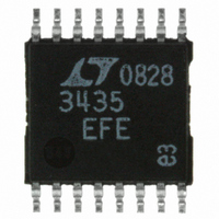
LT3435EFE#PBF Linear Technology, LT3435EFE#PBF Datasheet - Page 6

LT3435EFE#PBF
Manufacturer Part Number
LT3435EFE#PBF
Description
IC REG SW HV 3A 500KHZ 16-TSSOP
Manufacturer
Linear Technology
Type
Step-Down (Buck)r
Datasheet
1.LT3435EFEPBF.pdf
(24 pages)
Specifications of LT3435EFE#PBF
Internal Switch(s)
Yes
Synchronous Rectifier
No
Number Of Outputs
1
Voltage - Output
1.25 ~ 54 V
Current - Output
3A
Frequency - Switching
500kHz
Voltage - Input
3.3 ~ 60 V
Operating Temperature
-40°C ~ 125°C
Mounting Type
Surface Mount
Package / Case
16-TSSOP Exposed Pad, 16-eTSSOP, 16-HTSSOP
Primary Input Voltage
60V
No. Of Outputs
1
Output Voltage
68V
Output Current
2.4A
No. Of Pins
16
Operating Temperature Range
-40°C To +125°C
Msl
MSL 1 - Unlimited
Rohs Compliant
Yes
Lead Free Status / RoHS Status
Lead free / RoHS Compliant
Power - Output
-
Available stocks
Company
Part Number
Manufacturer
Quantity
Price
AC-COUPLED
500mA/DIV
50mV/DIV
PI FU CTIO S
LT3435
NC (Pin 1): No Connection.
SW (Pins 2, 5): The SW pin is the emitter of the on-chip
power NPN switch. This pin is driven up to the input pin
voltage during switch on time. Inductor current drives the
SW pin negative during switch off time. Negative voltage
is clamped with the external catch diode. Maximum nega-
tive switch voltage allowed is –0.8V.
V
NPN switch. V
a voltage on the BIAS pin is not present. High di/dt edges
occur on this pin during switch turn on and off. Keep the
path short from the V
capacitor, through the catch diode back to SW. All trace
6
TYPICAL PERFOR A CE CHARACTERISTICS
V
IN
I
OUT
4.0
3.5
3.0
2.5
2.0
1.5
1.0
0.5
SW
U
0
(Pins 3, 4): This is the collector of the on-chip power
2
Burst Mode Operation
V
V
Dropout Operation
V
BOOST DIODE = DIODES INC DFLS160
IN
OUT
OUT
= 12V
2.5
= 3.3V
= 3.3V
U
3
LOAD CURRENT = 2.5A
INPUT VOLTAGE (V)
IN
3.5
LOAD CURRENT = 250mA
powers the internal control circuitry when
10µs/DIV
4
U
4.5
IN
pin through the input bypass
5
W
5.5
3435 G22
3435 G19
U
6
AC-COUPLED
200mV/DIV
1A/DIV
V
I
OUT
OUT
6
5
4
3
2
1
0
2 2.5 3 3.5 4 4.5 5 5.5
No Load 2A Step Response
V
V
C
Dropout Operation
IN
OUT
OUT
V
BOOST DIODE = DIODES INC DFLS160
OUT
= 12V
= 3.3V
= 100µF
= 5V
INPUT VOLTAGE (V)
LOAD CURRENT = 250mA
500µs/DIV
LOAD CURRENT = 2.5A
inductance on this path will create a voltage spike at switch
off, adding to the V
BOOST (Pin 6): The BOOST pin is used to provide a drive
voltage, higher than the input voltage, to the internal
bipolar NPN power switch. Without this added voltage, the
typical switch voltage loss would be about 1.5V. The
additional BOOST voltage allows the switch to saturate
and its voltage loss approximates that of a 0.1Ω FET
structure.
C
of delay time between the PGFB pin exceeding its thresh-
old (V
T
(Pin 7): A capacitor on the C
PGFB
6
6.5 7 7.5
) and the PG pin set to a high impedance state.
3435 G23
3435 G20
AC-COUPLED
AC-COUPLED
CE
500mA/DIV
200mV/DIV
50mV/DIV
voltage across the internal NPN.
1A/DIV
V
V
I
OUT
I
OUT
OUT
SW
Step Response
Burst Mode Operation
V
V
V
V
C
I
LOAD(DC)
IN
OUT
IN
OUT
OUT
T
= 12V
= 12V
= 3.3V
= 3.3V
= 100µF
pin determines the amount
= 500mA
500µs/DIV
10ms/DIV
3435fa
3435 G21
3435 G24


