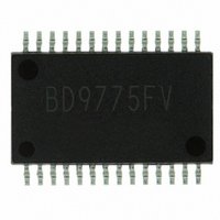
BD9775FV-E2 Rohm Semiconductor, BD9775FV-E2 Datasheet - Page 11

BD9775FV-E2
Manufacturer Part Number
BD9775FV-E2
Description
IC REG SW STEP DOWN HE 28-SSOP
Manufacturer
Rohm Semiconductor
Type
Step-Down (Buck)r
Specifications of BD9775FV-E2
Internal Switch(s)
No
Synchronous Rectifier
Yes
Number Of Outputs
2
Current - Output
400mA
Frequency - Switching
100kHz
Voltage - Input
6 ~ 30 V
Operating Temperature
-40°C ~ 85°C
Mounting Type
Surface Mount
Package / Case
28-SSOP
Power - Output
640mW
Mounting Style
SMD/SMT
Lead Free Status / RoHS Status
Lead free / RoHS Compliant
Voltage - Output
-
Lead Free Status / Rohs Status
Lead free / RoHS Compliant
Other names
BD9775FV-E2TR
Since ESR changes the phase characteristics, only one phase lead need be provided for high-ESR applications. Please choose
one of the following methods to add the phase lead.
When electrolytic or other high-ESR output capacitors are used:
When using ceramic, OS-CON, or other low-ESR capacitors for the output capacitor:
Ω). In DC/DC converter applications, where LC resonance circuits are always incorporated, the phase margin at these
locations is -180°. However, wherever ESR is present, a 90° phase lead is generated, limiting the net phase margin to -90°
in the presence of ESR. Since the desired phase margin is in a range less than 150°, this is a highly advantageous
approach in terms of the phase margin. However, it also has the drawback of increasing output voltage ripple components.
Phase compensation is relatively simple for applications employing high-ESR output capacitors (on the order of several
⑤ Add C to feedback resistor
⑦ Phase compensation provided by secondary (dual) phase lead
③ LC resonance circuit
Set the phase lead frequency close to the LC resonance frequency in order to cancel the LC resonance.
Where low-ESR (on the order of tens of mΩ) output capacitors are employed, a two phase-lead insertion scheme is
required, but this is different from the approach described in figure ③~⑥, since in this case the LC resonance gives rise
to a 180° phase margin/delay. Here, a phase compensation method such as that shown in figure ⑦ below can be
implemented.
Once the phase-lead frequency is determined, it should be set close to the LC resonance frequency.
This technique simplifies the phase topology of the DCDC Converter. Therefore, it might need a certain amount
of trial-and-error process. There are many factors(The PCB board layout, Output Current, etc.)that can affect
the DCDC characteristics. Please verify and confirm using practical applications.
Vo
fr =
Vo
Vcc
Resonance point phase margin -180°
Phase lead fz =
R1
R2
2π√LC
R1
R2
L
1
C1
C1
Fig-30
C
FB
[Hz]
Fig-32
Vo
2πC1R1
FB
R3
C2
A
1
Fig-28
A
C2
[Hz]
COMP
COMP
11/29
④ ESR connected
Phase lead fz1 =
Phase lead fz2 =
LC resonance frequency fr =
Vo
fr =
⑥ Add R3 to aggregator
Vcc
f
-90°:Pole
ESR
Phase lead fz =
resonance point1
=
R1
R2
2π√LC
2πR
L
C
1
ESR
C
R
ESR
Vo
2πR1C1
[Hz] :Zero
FB
2πR3C2
1
2πC2R3
R3
Fig-29
[Hz]:Resonance Point
1
A
1
2π√LC
C2
Fig-31
1
[Hz]
[Hz]
[Hz]
COMP
[Hz]


