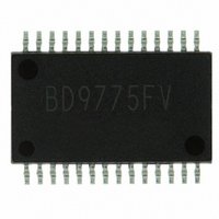
BD9775FV-E2 Rohm Semiconductor, BD9775FV-E2 Datasheet - Page 14

BD9775FV-E2
Manufacturer Part Number
BD9775FV-E2
Description
IC REG SW STEP DOWN HE 28-SSOP
Manufacturer
Rohm Semiconductor
Type
Step-Down (Buck)r
Specifications of BD9775FV-E2
Internal Switch(s)
No
Synchronous Rectifier
Yes
Number Of Outputs
2
Current - Output
400mA
Frequency - Switching
100kHz
Voltage - Input
6 ~ 30 V
Operating Temperature
-40°C ~ 85°C
Mounting Type
Surface Mount
Package / Case
28-SSOP
Power - Output
640mW
Mounting Style
SMD/SMT
Lead Free Status / RoHS Status
Lead free / RoHS Compliant
Voltage - Output
-
Lead Free Status / Rohs Status
Lead free / RoHS Compliant
Other names
BD9775FV-E2TR
●Operation notes
1)Absolute maximum ratings
2)GND electric potential
3)Thermal design
4)Inter-pin shorts and mounting errors
5)Operation in strong electromagnetic fields
6)Testing on application boards
7) The output FET
8)This monolithic IC contains P+ isolation and P substrate layers between adjacent elements in order to keep them isolated.
9)GND wiring pattern
(PINA)
When both a small-signal GND and high current GND are present, single-point grounding (at the set standard point) is
recommended, in order to separate the small-signal and high current patterns, and to be sure voltage changes stemming
from the wiring resistance and high current do not cause any voltage change in the small-signal GND. In the same way, care
must be taken to avoid wiring pattern fluctuations in any connected external component GND.
N
P
The shoot-through may happen when the input parasitic capacitance of FET is extremely big or the Duty ratio is less than
or equal to 10%. Less than or equal to 1000pF input parasitic capacitance is recommended. Please confirm operation on
the actual application since this character is affected by PCB layout and components.
Exceeding the absolute maximum ratings for supply voltage, operating temperature or other parameters can damage or
destroy the IC. When this occurs, it is impossible to identify the source of the damage as a short circuit, open circuit, etc.
Therefore, if any special mode is being considered with values expected to exceed absolute maximum ratings, consider
taking physical safety measures to protect the circuits, such as adding fuses.
Keep the GND terminal potential at the lowest (minimum) potential under any operating condition.
Be sure that the thermal design allows sufficient margin for power dissipation (Pd) under actual operating conditions.
Use caution when positioning the IC for mounting on printed surface boards. Connection errors may result in damage or
destruction of the IC. The IC can also be damaged when foreign substances short output pins together, or cause shorts
between the power supply and GND.
Use caution when operating in the presence of strong electromagnetic fields, as this may cause the IC to malfunction.
Connecting a capacitor to a low impedance pin for testing on an application board may subject the IC to stress. Be sure to
discharge the capacitors after every test process or step. Always turn the IC power supply off before connecting it to or
removing it from any of the apparatus used during the testing process. In addition, ground the IC during all steps in the
assembly process, and take similar antistatic precautions when transporting or storing the IC.
P-N junctions are formed at the intersection of these P layers with the N layers of other elements, creating a parasitic diode
or transistor. Relations between each potential may form as shown in the example below, where a resistor and transistor
are connected to a pin:
Parasitic diodes inevitably occur in the structure of the IC. Their operation can result in mutual interference between circuits,
and can cause malfunctions, and, in turn, physical damage or destruction. Therefore, do not employ any of the methods
under which parasitic diodes can operate, such as applying a voltage to an input pin lower than the (P substrate) GND.
P
○ With the resistor, when GND> Pin A, and with the transistor (NPN), when GND>Pin B:
○ With the transistor (NPN), when GND> Pin B:
+
The P-N junction operates as a parasitic diode
The P-N junction operates as a parasitic transistor by interacting with the N layers of elements in proximity to the
parasitic diode described above.
Resistor
Fig-37
N
GND
P
Parasitic element
P
+
(PINB)
N
Parasitic element or transistor
P
+
C
Transistor(NPN)
P substrate
Fig-38
N
B
GND
P
E
14/29
P
+
N
Parasitic element or transistor
(PINB)
Fig-39
B
C
E
GND
(PINA)
Parasitic element
Fig-40


