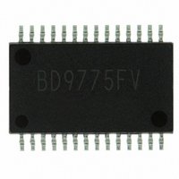
BD9775FV-E2 Rohm Semiconductor, BD9775FV-E2 Datasheet - Page 15

BD9775FV-E2
Manufacturer Part Number
BD9775FV-E2
Description
IC REG SW STEP DOWN HE 28-SSOP
Manufacturer
Rohm Semiconductor
Type
Step-Down (Buck)r
Specifications of BD9775FV-E2
Internal Switch(s)
No
Synchronous Rectifier
Yes
Number Of Outputs
2
Current - Output
400mA
Frequency - Switching
100kHz
Voltage - Input
6 ~ 30 V
Operating Temperature
-40°C ~ 85°C
Mounting Type
Surface Mount
Package / Case
28-SSOP
Power - Output
640mW
Mounting Style
SMD/SMT
Lead Free Status / RoHS Status
Lead free / RoHS Compliant
Voltage - Output
-
Lead Free Status / Rohs Status
Lead free / RoHS Compliant
Other names
BD9775FV-E2TR
13)Dropout operation
11)Thermal shutdown (TSD)
12)The SW pin
10)In some application and process testing, Vcc and pin potential may be reversed, possibly causing internal circuit or element
damage. For example, when the external capacitor is charged, the electric charge can cause a Vcc short circuit to the GND.
In order to avoid these problems, limiting output pin capacitance to 100μF or less and inserting a Vcc series countercurrent
prevention diode or bypass diode between the various pins and the Vcc is recommended.
This IC is provided with a built-in thermal shutdown (TSD) circuit, which is designed to prevent thermal damage to or
destruction of the IC. Normal operation should be within the power dissipation parameter, but if the IC should run beyond
allowable Pd for a continued period, junction temperature (Tj) will rise, thus activating the TSD circuit, and turning all output
pins OFF. When Tj again falls below the TSD threshold, circuits are automatically restored to normal operation. Note that
the TSD circuit is only asserted beyond the absolute maximum rating. Therefore, under no circumstances should the TSD
be used in set design or for any purpose other than protecting the IC against overheating
When the SW pin is connected in an application, its coil counter-electromotive force may give rise to a single electric
potential. When setting up the application, make sure that the SW pin never exceeds the absolute maximum value.
Connecting a resistor of several Ω will reduce the electric potential. (See Fig. 43)
When input voltage falls below approximately output voltage / 0.9 (varying depending on operating frequency) the ON
interval on the OUTL side MOS is lost, making boost applications and wrap operation impossible. If a small differential
between input and output voltage is envisioned for a prospective application, connect the load such that the SW voltage
drops to the GND level. Managing this load requires discharging the SW line capacitance (SW pin capacitance: approx.
500pF; OUTL side MOS D-S capacitance; Schottky capacitance). Supported loads can be calculated using the equation
below.
Note that SW line capacitance is lower with smaller loads, and more stable operation is attained when low voltage bias
circuits are configured as in the example below (Fig. 44). However, the degree to which line capacitance is reduced or
operational stability is attained will vary depending on the board layout and components. Therefore, be certain to confirm
the effectiveness of these design factors in actual operation before entering mass production.
Countercurrent prevention diode
OUT
OUT
SW
ILOAD =
Vcc
BOOT
OUTH
SW
OUTL
DGND
Output voltage × SW line capacitance
R
15/29
Vcc
Fig-43
Vcc
Pin
Vo
25n
VREG
Vo
Bypass diode
Fig-41
Fig-42
Vcc


