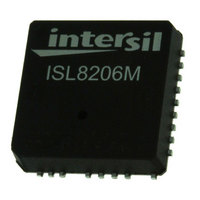
ISL8206MIRZ Intersil, ISL8206MIRZ Datasheet - Page 3

ISL8206MIRZ
Manufacturer Part Number
ISL8206MIRZ
Description
IC BUCK SYNC ADJ 6A 15QFN
Manufacturer
Intersil
Type
Step-Down (Buck)r
Datasheet
1.ISL8204MIRZ.pdf
(20 pages)
Specifications of ISL8206MIRZ
Internal Switch(s)
Yes
Synchronous Rectifier
Yes
Number Of Outputs
1
Voltage - Output
0.6 ~ 6 V
Current - Output
6A
Frequency - Switching
600kHz
Voltage - Input
1 ~ 20 V
Operating Temperature
-40°C ~ 85°C
Mounting Type
Surface Mount
Package / Case
15-QFN
Lead Free Status / RoHS Status
Lead free / RoHS Compliant
Power - Output
-
Available stocks
Company
Part Number
Manufacturer
Quantity
Price
Company:
Part Number:
ISL8206MIRZ
Manufacturer:
intersil10
Quantity:
331
Company:
Part Number:
ISL8206MIRZ-T
Manufacturer:
Intersil
Quantity:
500
Pin Configuration
Pin Descriptions
PHASE
1, 2, 3, 4
6, 8, 15
PIN
10
11
12
10
5
7
9
9
PD1
SYMBOL
(PD1)
PHASE
(PD2)
(PD3)
(PD4)
PGND
PGND
VOUT
PVCC
ISET
VIN
NC
8
PD2
7
11
3
Power ground pin for signal, input, and output return path. PGND needs to connect to one (or more)
ground plane(s) immediately, which is recommended to minimize the effect of switching noise, copper
losses, and maximize heat dissipation. Range: 0V.
This pin provides the bias supply for ISL8204M, ISL8206M, as well as the low-side MOSFET’s gate and
high-side MOSFET’s gate. If PVCC rises above 6.5V, an internal 5V regulator will supply to the internal
logics bias (but high-side and low-side MOSFET gate will still be sourced by PVCC). Connect a well
decoupled +5V or +12V supply to this pin. Connect 1µF ceramic capacitor to ground plane directly.
Range: 4.5V to 14.4V.
No internal connection.
The ISET pin is the input for the overcurrent protection (OCP) setting, which compares the r
the low-side MOSFET to set the overcurrent threshold. The ISL8204M, ISL8206M has an initial protect
overcurrent limit. It has an integrated internal 4.12kΩ/2.87kΩ resistor (R
and PGND pins, which can prevent significant overcurrent impact to the module. One can also
connect an additional resistor R
current limit point by paralleling. Range: 0 to PVCC.
Power input pin. Apply input voltage between the VIN pin and PGND pin. It is recommended to place
an input decoupling capacitor directly between the VIN pin and the PGND pin. The input capacitor
should be placed as closely as possible to the module. Range: 1V to 20V.
The PHASE pin is the switching node between the high and low side MOSFET. It also returns the current
path for the high side MOSFET driver and detects the low-side MOSFET drain voltage for the
overcurrent limits point. Range: 0V to 30V.
Power ground pin for signal, input, and output return path. PGND needs to connect to one (or more)
ground plane(s) immediately, which is recommended to minimize the effect of switching noise, copper
losses, and maximize heat dissipation. Range: 0V.
Power output pin. Apply output load between this pin and the PGND pin. It is recommended to place
a high frequency output decoupling capacitor directly between the VOUT pin and the PGND pin. The
output capacitor should be placed as closely as possible to the module. Range: 0.6V to 6V.
6
PD3
PGND
5
4
3
ISL8204M, ISL8206M
PD4
2
ISL8204M, ISL8206M
TOP AND 3D VIEW
(15 LD QFN)
1
15
14
13
12
SET-EX
PGND
NC
FB
COMP/EN
VOUT
between the ISET pin and the PGND pin in order to reduce the
DESCRIPTION
SET-IN
) between the ISET
December 16, 2010
DS(ON)
FN6999.2
of


