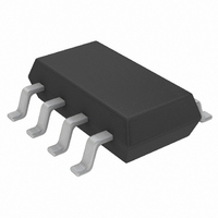
LTC3872ETS8#TRMPBF Linear Technology, LTC3872ETS8#TRMPBF Datasheet - Page 11

LTC3872ETS8#TRMPBF
Manufacturer Part Number
LTC3872ETS8#TRMPBF
Description
IC DC/DC CNTRLR TSOT23-8
Manufacturer
Linear Technology
Type
Step-Up (Boost)r
Datasheet
1.LTC3872ETS8TRMPBF.pdf
(22 pages)
Specifications of LTC3872ETS8#TRMPBF
Internal Switch(s)
No
Synchronous Rectifier
No
Number Of Outputs
1
Voltage - Output
1.2 ~ 60 V
Current - Output
10A
Frequency - Switching
550kHz
Voltage - Input
2.75 ~ 9.8 V
Operating Temperature
-40°C ~ 85°C
Mounting Type
Surface Mount
Package / Case
TSOT-23-8, TSOT-8
Primary Input Voltage
9.8V
No. Of Outputs
1
Output Voltage
60V
No. Of Pins
8
Operating Temperature Range
-40°C To +85°C
Msl
MSL 1 - Unlimited
Supply Voltage Range
2.75V To 9.8V
Rohs Compliant
Yes
Lead Free Status / RoHS Status
Lead free / RoHS Compliant
Power - Output
-
Other names
LTC3872ETS8#TRMPBF
LTC3872ETS8#TRMPBFTR
LTC3872ETS8#TRMPBFTR
Available stocks
Company
Part Number
Manufacturer
Quantity
Price
Calculating Power MOSFET Switching and Conduction
Losses and Junction Temperatures
In order to calculate the junction temperature of the power
MOSFET, the power dissipated by the device must be known.
This power dissipation is a function of the duty cycle, the
load current and the junction temperature itself (due to
the positive temperature coefficient of its R
result, some iterative calculation is normally required to
determine a reasonably accurate value. Since the controller
is using the MOSFET as both a switching and a sensing
element, care should be taken to ensure that the converter
is capable of delivering the required load current over all
operating conditions (line voltage and temperature), and
for the worst-case specifications for V
R
sheet.
The power dissipated by the MOSFET in a boost converter is:
The first term in the equation above represents the I
losses in the device, and the second term, the switching
losses. The constant, k = 1.7, is an empirical factor inversely
related to the gate drive current and has the dimension
of 1/current.
From a known power dissipated in the power MOSFET, its
junction temperature can be obtained using the following
formula:
The R
the R
the case to the ambient temperature (R
of T
used in the iterative calculation process.
Output Diode Selection
To maximize efficiency, a fast switching diode with low
forward drop and low reverse leakage is desired. The output
applicaTions inForMaTion
DS(ON)
T
P
J
J
FET
TH(JC)
can then be compared to the original, assumed value
= T
TH(JA)
+k • V
of the MOSFET listed in the manufacturer’s data
=
A
+ P
for the device plus the thermal resistance from
to be used in this equation normally includes
1– D
I
O(MAX)
FET
O
1.85
MAX
• R
TH(JA)
•
(
1– D
2
I
O(MAX)
• R
MAX
DS(ON)
)
• C
• D
RSS
SENSE(MAX)
MAX
TH(CA)
• f
• ρ
DS(ON)
). This value
T
and the
). As a
2
R
diode in a boost converter conducts current during the
switch off-time. The peak reverse voltage that the diode
must withstand is equal to the regulator output voltage.
The average forward current in normal operation is equal
to the output current, and the peak current is equal to the
peak inductor current.
The power dissipated by the diode is:
and the diode junction temperature is:
The R
the R
the board to the ambient temperature in the enclosure.
Remember to keep the diode lead lengths short and to
observe proper switch-node layout (see Board Layout
Checklist) to avoid excessive ringing and increased dis-
sipation.
Output Capacitor Selection
Contributions of ESR (equivalent series resistance), ESL
(equivalent series inductance) and the bulk capacitance
must be considered when choosing the correct component
for a given output ripple voltage. The effects of these three
parameters (ESR, ESL and bulk C) on the output voltage
ripple waveform are illustrated in Figure 6e for a typical
boost converter.
The choice of component(s) begins with the maximum
acceptable ripple voltage (expressed as a percentage of
the output voltage), and how this ripple should be divided
between the ESR step and the charging/discharging DV.
For the purpose of simplicity we will choose 2% for the
maximum output ripple, to be divided equally between the
ESR step and the charging/discharging DV. This percentage
ripple will change, depending on the requirements of the
application, and the equations provided below can easily
be modified.
P
T
I
D(PEAK)
J
D
TH(JC)
= T
TH(JA)
= I
O(MAX)
A
+ P
=I
for the device plus the thermal resistance from
to be used in this equation normally includes
L(PEAK)
D
• V
• R
D
TH(JA)
= 1+
χ
2
•
1– D
I
O(MAX)
MAX
LTC3872
11
3872fb


