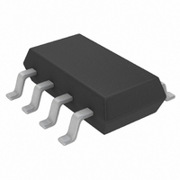
LTC3872ETS8#TRMPBF Linear Technology, LTC3872ETS8#TRMPBF Datasheet - Page 14

LTC3872ETS8#TRMPBF
Manufacturer Part Number
LTC3872ETS8#TRMPBF
Description
IC DC/DC CNTRLR TSOT23-8
Manufacturer
Linear Technology
Type
Step-Up (Boost)r
Datasheet
1.LTC3872ETS8TRMPBF.pdf
(22 pages)
Specifications of LTC3872ETS8#TRMPBF
Internal Switch(s)
No
Synchronous Rectifier
No
Number Of Outputs
1
Voltage - Output
1.2 ~ 60 V
Current - Output
10A
Frequency - Switching
550kHz
Voltage - Input
2.75 ~ 9.8 V
Operating Temperature
-40°C ~ 85°C
Mounting Type
Surface Mount
Package / Case
TSOT-23-8, TSOT-8
Primary Input Voltage
9.8V
No. Of Outputs
1
Output Voltage
60V
No. Of Pins
8
Operating Temperature Range
-40°C To +85°C
Msl
MSL 1 - Unlimited
Supply Voltage Range
2.75V To 9.8V
Rohs Compliant
Yes
Lead Free Status / RoHS Status
Lead free / RoHS Compliant
Power - Output
-
Other names
LTC3872ETS8#TRMPBF
LTC3872ETS8#TRMPBFTR
LTC3872ETS8#TRMPBFTR
Available stocks
Company
Part Number
Manufacturer
Quantity
Price
output current. Assuming an efficiency of 90%, this
sense resistor power dissipation represents 1.3% of the
overall input power. In other words, for this application,
the use of V
approximately 1.3%.
For more details regarding the various terms in these
equations, please refer to the section Boost Converter:
Power MOSFET Selection.
3. The losses in the inductor are simply the DC input cur-
rent squared times the winding resistance. Expressing this
loss as a function of the output current yields:
4. Losses in the boost diode. The power dissipation in the
boost diode is:
The boost diode can be a major source of power loss in
a boost converter. For the 3.3V input, 5V output at 7A ex-
ample given above, a Schottky diode with a 0.4V forward
voltage would dissipate 2.8W, which represents 7% of the
input power. Diode losses can become significant at low
output voltages where the forward voltage is a significant
percentage of the output voltage.
5. Other losses, including C
inductor core losses, generally account for less than 2%
of the total additional loss.
Checking Transient Response
The regulator loop response can be verified by looking at
the load transient response. Switching regulators generally
take several cycles to respond to an instantaneous step
in resistive load current. When the load step occurs, V
immediately shifts by an amount equal to (DI
and then C
the direction of the load step) as shown in Figure 7. The
regulator feedback loop acts on the resulting error amp
output signal to return V
this recovery time, V
ringing that would indicate a stability problem.
LTC3872
applicaTions inForMaTion
14
P
P
DIODE
R(WINDING)
= I
O
begins to charge or discharge (depending on
DS
O(MAX)
sensing would increase the efficiency by
=
1– D
• V
O
I
O(MAX)
can be monitored for overshoot or
D
O
MAX
to its steady-state value. During
IN
and C
2
• R
O
W
ESR dissipation and
LOAD
)(ESR),
O
A second, more severe transient can occur when con-
necting loads with large (>1µF) supply bypass capacitors.
The discharged bypass capacitors are effectively put in
parallel with C
this problem if the load switch resistance is low and it is
driven quickly. The only solution is to limit the rise time
of the switch drive in order to limit the inrush current
di/dt to the load.
Boost Converter Design Example
The design example given here will be for the circuit shown
on the front page. The input voltage is 3.3V, and the output
is 5V at a maximum load current of 2A.
1. The duty cycle is:
2. An inductor ripple current of 40% of the maximum load
current is chosen, so the peak input current (which is also
the minimum saturation current) is:
The inductor ripple current is:
V
I
IN(PEAK)
O
. No regulator can deliver enough current to prevent
D =
∆I
AC-COUPLED
L
200mV/DIV
500mA/DIV
Figure 7. Load Transient Response for a 3.3V Input,
5V Output Boost Converter Application, 0.1A to 1A Step
= χ •
V
V
= 1+
OUT
O
I
V
L
+ V
1– D
I
O
O(MAX)
O
+ V
, causing a nearly instantaneous drop in
D
χ
2
MAX
– V
D
•
IN
1– D
= 0.4 •
I
O(MAX)
=
MAX
5 + 0.4 – 3.3
20µs/DIV
1– 0.39
5 + 0.4
= 1.2 •
2
= 1.3A
1– 0. 39
= 38.9%
2
3872 F07
= 3.9A
3872fb


