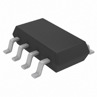
LTC3872ETS8#TRMPBF Linear Technology, LTC3872ETS8#TRMPBF Datasheet - Page 15

LTC3872ETS8#TRMPBF
Manufacturer Part Number
LTC3872ETS8#TRMPBF
Description
IC DC/DC CNTRLR TSOT23-8
Manufacturer
Linear Technology
Type
Step-Up (Boost)r
Datasheet
1.LTC3872ETS8TRMPBF.pdf
(22 pages)
Specifications of LTC3872ETS8#TRMPBF
Internal Switch(s)
No
Synchronous Rectifier
No
Number Of Outputs
1
Voltage - Output
1.2 ~ 60 V
Current - Output
10A
Frequency - Switching
550kHz
Voltage - Input
2.75 ~ 9.8 V
Operating Temperature
-40°C ~ 85°C
Mounting Type
Surface Mount
Package / Case
TSOT-23-8, TSOT-8
Primary Input Voltage
9.8V
No. Of Outputs
1
Output Voltage
60V
No. Of Pins
8
Operating Temperature Range
-40°C To +85°C
Msl
MSL 1 - Unlimited
Supply Voltage Range
2.75V To 9.8V
Rohs Compliant
Yes
Lead Free Status / RoHS Status
Lead free / RoHS Compliant
Power - Output
-
Other names
LTC3872ETS8#TRMPBF
LTC3872ETS8#TRMPBFTR
LTC3872ETS8#TRMPBFTR
Available stocks
Company
Part Number
Manufacturer
Quantity
Price
And so the inductor value is:
The component chosen is a 2.2µH inductor made by
Sumida (part number CEP125-H 1ROMH).
3. Assuming a MOSFET junction temperature of 125°C,
the room temperature MOSFET R
than:
The MOSFET used was the Si3460, which has a maximum
R
30V, and a gate charge of 13.5nC at 4.5V V
4. The diode for this design must handle a maximum DC
output current of 2A and be rated for a minimum reverse
voltage of V
conductor (MBRB2515L) was chosen for its high power
dissipation capability.
5. The output capacitor usually consists of a lower valued,
low ESR ceramic.
applicaTions inForMaTion
DS(ON)
L =
R
= 0.175V •
DS(ON)
V
∆I
IN(MIN)
of 27mΩ at 4.5V V
L
≤ V
• f
OUT
SENSE(MAX)
• D
, or 5V. A 25A, 15V diode from On Semi-
1+
MAX
0.4
1– 0.39
2
=
• 2A • 1.5
1.3A • 550kHz
•
BOLD LINES INDICATE HIGH CURRENT PATHS
R
GS
ITH
C
1+
Figure 8. LTC3872 Layout Diagram (See PC Board Layout Checklist)
3.3V
ITH
, a BV
χ
2
R1
1– D
DS(ON)
≈ 30mΩ
•I
DSS
O(MAX)
MAX
• 0.39 = 1.8µH
of greater than
should be less
IPRG
I
V
GND
TH
FB
GS
.
• ρ
LTC3872
R2
T
RUN/SS
NGATE
SW
V
IN
6. The choice of an input capacitor for a boost converter
depends on the impedance of the source supply and the
amount of input ripple the converter will safely tolerate.
For this particular design two 22µF Taiyo Yuden ceramic
capacitors (JMK325BJ226MM) is required (the input
and return lead lengths are kept to a few inches. As with
the output node, check the input ripple with a single
oscilloscope probe connected across the input capacitor
terminals.
PC Board Layout Checklist
When laying out the printed circuit board, the following
checklist should be used to ensure proper operation of
the LTC3872. These items are illustrated graphically in
the layout diagram in Figure 8. Check the following in
your layout:
1. The Schottky diode should be closely connected between
the output capacitor and the drain of the external MOSFET.
2. The input decoupling capacitor (0.1µF) should be con-
nected closely between V
3. The trace from SW to the switch point should be kept
short.
4. Keep the switching node NGATE away from sensitive
small signal nodes.
5. The V
resistors. The resistive divider R1 and R2 must be con-
nected between the (+) plate of C
+
FB
C
IN
L1
pin should connect directly to the feedback
+
D1
C
OUT
3872 F08
IN
M1
and GND.
V
V
OUT
IN
OUT
and signal ground.
LTC3872
15
3872fb


