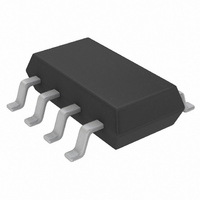
LTC3872ETS8#TRMPBF Linear Technology, LTC3872ETS8#TRMPBF Datasheet - Page 9

LTC3872ETS8#TRMPBF
Manufacturer Part Number
LTC3872ETS8#TRMPBF
Description
IC DC/DC CNTRLR TSOT23-8
Manufacturer
Linear Technology
Type
Step-Up (Boost)r
Datasheet
1.LTC3872ETS8TRMPBF.pdf
(22 pages)
Specifications of LTC3872ETS8#TRMPBF
Internal Switch(s)
No
Synchronous Rectifier
No
Number Of Outputs
1
Voltage - Output
1.2 ~ 60 V
Current - Output
10A
Frequency - Switching
550kHz
Voltage - Input
2.75 ~ 9.8 V
Operating Temperature
-40°C ~ 85°C
Mounting Type
Surface Mount
Package / Case
TSOT-23-8, TSOT-8
Primary Input Voltage
9.8V
No. Of Outputs
1
Output Voltage
60V
No. Of Pins
8
Operating Temperature Range
-40°C To +85°C
Msl
MSL 1 - Unlimited
Supply Voltage Range
2.75V To 9.8V
Rohs Compliant
Yes
Lead Free Status / RoHS Status
Lead free / RoHS Compliant
Power - Output
-
Other names
LTC3872ETS8#TRMPBF
LTC3872ETS8#TRMPBFTR
LTC3872ETS8#TRMPBFTR
Available stocks
Company
Part Number
Manufacturer
Quantity
Price
the inductor value can be determined using the following
equation:
Remember that boost converters are not short-circuit
protected. Under a shorted output condition, the induc-
tor current is limited only by the input supply capability.
The minimum required saturation current of the inductor
can be expressed as a function of the duty cycle and the
load current, as follows:
The saturation current rating for the inductor should be
checked at the minimum input voltage (which results in
the highest inductor current) and maximum output current.
Operating in Discontinuous Mode
Discontinuous mode operation occurs when the load cur-
rent is low enough to allow the inductor current to run
out during the off-time of the switch. Once the inductor
current is near zero, the switch and diode capacitances
resonate with the inductance to form damped ringing at
1MHz to 10MHz. If the off-time is long enough, the drain
voltage will settle to the input voltage.
Depending on the input voltage and the residual energy
in the inductor, this ringing can cause the drain of the
power MOSFET to go below ground where it is clamped
by the body diode. This ringing is not harmful to the IC
and it has been shown not to contribute significantly to
EMI. Any attempt to damp it with a snubber will degrade
the efficiency.
Inductor Core Selection
Once the value for L is known, the type of inductor must
be selected. Actual core loss is independent of core size
for a fixed inductor value, but is very dependent on the
applicaTions inForMaTion
I
where:
L(SAT)
L =
∆I
L
V
= χ •
≥ 1+
∆I
IN(MIN)
L
• f
1– D
I
O(MAX)
χ
2
• D
MAX
•
MAX
1– D
I
O(MAX)
MAX
inductance selected. As inductance increases, core losses
go down. Unfortunately, increased inductance requires
more turns of wire and therefore, copper losses will in-
crease. Generally, there is a tradeoff between core losses
and copper losses that needs to be balanced.
Ferrite designs have very low core losses and are pre-
ferred at high switching frequencies, so design goals can
concentrate on copper losses and preventing saturation.
Ferrite core material saturates “hard,” meaning that the
inductance collapses rapidly when the peak design current
is exceeded. This results in an abrupt increase in inductor
ripple current and consequently, output voltage ripple. Do
not allow the core to saturate!
Different core materials and shapes will change the size/
current and price/current relationship of an inductor. Toroid
or shielded pot cores in ferrite or permalloy materials are
small and don’t radiate much energy, but generally cost
more than powdered iron core inductors with similar
characteristics. The choice of which style inductor to use
mainly depends on the price vs size requirements and any
radiated field/EMI requirements. New designs for surface
mount inductors are available from Coiltronics, Coilcraft,
Toko and Sumida.
Power MOSFET Selection
The power MOSFET serves two purposes in the LTC3872:
it represents the main switching element in the power
path and its R
ment for the control loop. Important parameters for the
power MOSFET include the drain-to-source breakdown
voltage (BV
resistance (R
gate-to-source and gate-to-drain charges (Q
respectively), the maximum drain current (I
the MOSFET’s thermal resistances (R
Logic-level (4.5V V
be used when input voltage is high, otherwise if low input
voltage operation is expected (e.g., supplying power from
a lithium-ion battery or a 3.3V logic supply), then sublogic-
level (2.5V V
Pay close attention to the BV
MOSFETs relative to the maximum actual switch voltage
in the application. Many logic-level devices are limited
DSS
GS-RATED
DS(ON)
DS(ON)
), the threshold voltage (V
GS-RATED
) versus gate-to-source voltage, the
) threshold MOSFETs should be used.
represents the current sensing ele-
) threshold MOSFETs should
DSS
specifications for the
TH(JC)
LTC3872
GS(TH)
and R
GS
D(MAX)
), the on-
and Q
TH(JA)
) and
3872fb
9
GD
).
,


