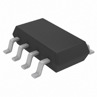
LTC3872ETS8#TRMPBF Linear Technology, LTC3872ETS8#TRMPBF Datasheet - Page 8

LTC3872ETS8#TRMPBF
Manufacturer Part Number
LTC3872ETS8#TRMPBF
Description
IC DC/DC CNTRLR TSOT23-8
Manufacturer
Linear Technology
Type
Step-Up (Boost)r
Datasheet
1.LTC3872ETS8TRMPBF.pdf
(22 pages)
Specifications of LTC3872ETS8#TRMPBF
Internal Switch(s)
No
Synchronous Rectifier
No
Number Of Outputs
1
Voltage - Output
1.2 ~ 60 V
Current - Output
10A
Frequency - Switching
550kHz
Voltage - Input
2.75 ~ 9.8 V
Operating Temperature
-40°C ~ 85°C
Mounting Type
Surface Mount
Package / Case
TSOT-23-8, TSOT-8
Primary Input Voltage
9.8V
No. Of Outputs
1
Output Voltage
60V
No. Of Pins
8
Operating Temperature Range
-40°C To +85°C
Msl
MSL 1 - Unlimited
Supply Voltage Range
2.75V To 9.8V
Rohs Compliant
Yes
Lead Free Status / RoHS Status
Lead free / RoHS Compliant
Power - Output
-
Other names
LTC3872ETS8#TRMPBF
LTC3872ETS8#TRMPBFTR
LTC3872ETS8#TRMPBFTR
Available stocks
Company
Part Number
Manufacturer
Quantity
Price
Output Voltage Programming
The output voltage is set by a resistor divider according
to the following formula:
The external resistor divider is connected to the output
as shown in the Typical Application on the front page,
allowing remote voltage sensing.
Application Circuits
A basic LTC3872 application circuit is shown on the front
page of this datasheet. External component selection is
driven by the characteristics of the load and the input supply.
Duty Cycle Considerations
For a boost converter operating in a continuous conduc-
tion mode (CCM), the duty cycle of the main switch is:
where V
converters where the input voltage is close to the output
voltage, the duty cycle is low and for converters that develop
a high output voltage from a low voltage input supply, the
duty cycle is high. The LTC3872 has a built-in circuit that
allows the extension of the maximum duty cycle while
keeping the minimum switch off time unchanged. This
is accomplished by reducing the clock frequency when
the duty cycle is close to 80%. This function allows the
user to obtain high output voltages from low input supply
voltages. The shift of frequency with duty cycle is shown
in the Typical Performance Characteristics section.
The Peak and Average Input Currents
The control circuit in the LTC3872 is measuring the input
current (either by using the R
or by using a sense resistor in the MOSFET source), so
the output current needs to be reflected back to the input
in order to dimension the power MOSFET properly. Based
LTC3872
applicaTions inForMaTion
8
D =
V
O
= 1.2V • 1+
D
V
O
is the forward voltage of the boost diode. For
V
+ V
O
+ V
D
– V
D
R2
R1
IN
DS(ON)
of the power MOSFET
on the fact that, ideally, the output power is equal to the
input power, the maximum average input current is:
Ripple Current I
The constant c in the equation above represents the
percentage peak-to-peak ripple current in the inductor,
relative to its maximum value. For example, if 30% ripple
current is chosen, then c = 0.30, and the peak current is
15% greater than the average.
For a current mode boost regulator operating in CCM,
slope compensation must be added for duty cycles above
50% in order to avoid subharmonic oscillation. For the
LTC3872, this ramp compensation is internal. Having an
internally fixed ramp compensation waveform, however,
does place some constraints on the value of the inductor
and the operating frequency. If too large an inductor is
used, the resulting current ramp (I
to the internal ramp compensation (at duty cycles above
50%), and the converter operation will approach voltage
mode (ramp compensation reduces the gain of the current
loop). If too small an inductor is used, but the converter is
still operating in CCM (continuous conduction mode), the
internal ramp compensation may be inadequate to prevent
subharmonic oscillation. To ensure good current mode gain
and avoid subharmonic oscillation, it is recommended that
the ripple current in the inductor fall in the range of 20%
to 40% of the maximum average current. For example, if
the maximum average input current is 1A, choose an I
between 0.2A and 0.4A, and a value c between 0.2 and 0.4.
Inductor Selection
Given an operating input voltage range, and having chosen
the operating frequency and ripple current in the inductor,
The peak input current is:
I
I
IN(MAX)
IN(PEAK)
=
= 1+
1– D
I
O(MAX)
L
MAX
and the c Factor
χ
2
•
1– D
I
O(MAX)
MAX
L
) will be small relative
3872fb
L


