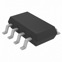
LTC3872ETS8#TRMPBF Linear Technology, LTC3872ETS8#TRMPBF Datasheet - Page 13

LTC3872ETS8#TRMPBF
Manufacturer Part Number
LTC3872ETS8#TRMPBF
Description
IC DC/DC CNTRLR TSOT23-8
Manufacturer
Linear Technology
Type
Step-Up (Boost)r
Datasheet
1.LTC3872ETS8TRMPBF.pdf
(22 pages)
Specifications of LTC3872ETS8#TRMPBF
Internal Switch(s)
No
Synchronous Rectifier
No
Number Of Outputs
1
Voltage - Output
1.2 ~ 60 V
Current - Output
10A
Frequency - Switching
550kHz
Voltage - Input
2.75 ~ 9.8 V
Operating Temperature
-40°C ~ 85°C
Mounting Type
Surface Mount
Package / Case
TSOT-23-8, TSOT-8
Primary Input Voltage
9.8V
No. Of Outputs
1
Output Voltage
60V
No. Of Pins
8
Operating Temperature Range
-40°C To +85°C
Msl
MSL 1 - Unlimited
Supply Voltage Range
2.75V To 9.8V
Rohs Compliant
Yes
Lead Free Status / RoHS Status
Lead free / RoHS Compliant
Power - Output
-
Other names
LTC3872ETS8#TRMPBF
LTC3872ETS8#TRMPBFTR
LTC3872ETS8#TRMPBFTR
Available stocks
Company
Part Number
Manufacturer
Quantity
Price
both available in surface mount packages. In the case of
tantalum, it is critical that the capacitors have been surge
tested for use in switching power supplies. An excellent
choice is AVX TPS series of surface mount tantalum. Also,
ceramic capacitors are now available with extremely low
ESR, ESL and high ripple current ratings.
Input Capacitor Selection
The input capacitor of a boost converter is less critical
than the output capacitor, due to the fact that the inductor
is in series with the input and the input current waveform
is continuous (see Figure 6b). The input voltage source
impedance determines the size of the input capacitor,
which is typically in the range of 10µF to 100µF . A low ESR
capacitor is recommended, although it is not as critical as
for the output capacitor.
The RMS input capacitor ripple current for a boost con-
verter is:
Please note that the input capacitor can see a very high
surge current when a battery is suddenly connected to
the input of the converter and solid tantalum capacitors
can fail catastrophically under these conditions. Be sure
to specify surge-tested capacitors!
Efficiency Considerations: How Much Does VDS
Sensing Help?
The efficiency of a switching regulator is equal to the output
power divided by the input power (×100%).
Percent efficiency can be expressed as:
where L1, L2, etc. are the individual loss components as a
percentage of the input power. It is often useful to analyze
individual losses to determine what is limiting the efficiency
and which change would produce the most improvement.
Although all dissipative elements in the circuit produce
losses, four main sources usually account for the majority
of the losses in LTC3872 application circuits:
1. The supply current into V
applicaTions inForMaTion
% Efficiency = 100% – (L1 + L2 + L3 + …),
I
RMS(CIN)
= 0.3 •
V
IN(MIN)
L • f
• D
IN
MAX
. The V
IN
current is the
sum of the DC supply current I
Characteristics) and the MOSFET driver and control cur-
rents. The DC supply current into the V
about 250µA and represents a small power loss (much
less than 1%) that increases with V
results from switching the gate capacitance of the power
MOSFET; this current is typically much larger than the DC
current. Each time the MOSFET is switched on and then
off, a packet of gate charge Q
to ground. The resulting dQ/dt is a current that must be
supplied to the Input capacitor by an external supply. If
the IC is operating in CCM:
2. Power MOSFET switching and conduction losses. The
technique of using the voltage drop across the power
MOSFET to close the current feedback loop was chosen
because of the increased efficiency that results from not
having a sense resistor. The losses in the power MOSFET
are equal to:
discrete sense resistor can be calculated almost by inspec-
tion.
To understand the magnitude of the improvement with
this V
output power supply shown in the Typical Application on
the front page. The maximum load current is 7A (10A peak)
and the duty cycle is 39%. Assuming a ripple current of
40%, the peak inductor current is 13.8A and the average
is 11.5A. With a maximum sense voltage of about 140mV,
the sense resistor value would be 10mΩ, and the power
dissipated in this resistor would be 514mW at maximum
I
P
The I
P
P
Q(TOT)
IC
FET
R(SENSE)
DS
= V
+ k • V
2
=
R power savings that result from not having a
sensing technique, consider the 3.3V input, 5V
IN
≈ I
1– D
• (I
Q
I
O(MAX)
=
O
= f • Q
Q
1.85
MAX
+ f • Q
1– D
I
O(MAX)
•
G
1– D
MAX
I
2
G
O(MAX)
)
• R
MAX
DS(ON)
2
• R
G
Q
• C
is transferred from V
SENSE
(given in the Electrical
RSS
• D
IN
. The driver current
MAX
LTC3872
• f
IN
• D
pin is typically
• ρ
MAX
T
13
3872fb
IN


