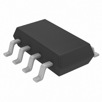
LTC3872ETS8#TRMPBF Linear Technology, LTC3872ETS8#TRMPBF Datasheet - Page 7

LTC3872ETS8#TRMPBF
Manufacturer Part Number
LTC3872ETS8#TRMPBF
Description
IC DC/DC CNTRLR TSOT23-8
Manufacturer
Linear Technology
Type
Step-Up (Boost)r
Datasheet
1.LTC3872ETS8TRMPBF.pdf
(22 pages)
Specifications of LTC3872ETS8#TRMPBF
Internal Switch(s)
No
Synchronous Rectifier
No
Number Of Outputs
1
Voltage - Output
1.2 ~ 60 V
Current - Output
10A
Frequency - Switching
550kHz
Voltage - Input
2.75 ~ 9.8 V
Operating Temperature
-40°C ~ 85°C
Mounting Type
Surface Mount
Package / Case
TSOT-23-8, TSOT-8
Primary Input Voltage
9.8V
No. Of Outputs
1
Output Voltage
60V
No. Of Pins
8
Operating Temperature Range
-40°C To +85°C
Msl
MSL 1 - Unlimited
Supply Voltage Range
2.75V To 9.8V
Rohs Compliant
Yes
Lead Free Status / RoHS Status
Lead free / RoHS Compliant
Power - Output
-
Other names
LTC3872ETS8#TRMPBF
LTC3872ETS8#TRMPBFTR
LTC3872ETS8#TRMPBFTR
Available stocks
Company
Part Number
Manufacturer
Quantity
Price
operaTion
Main Control Loop
The LTC3872 is a No R
mode controller for DC/DC boost, SEPIC and flyback
converter applications. The LTC3872 is distinguished from
conventional current mode controllers because the current
control loop can be closed by sensing the voltage drop
across the power MOSFET switch or across a discrete
sense resistor, as shown in Figures 1 and 2. This No R
sensing technique improves efficiency, increases power
density and reduces the cost of the overall solution.
For circuit operation, please refer to the Block Diagram
of the IC and the Typical Application on the front page. In
normal operation, the power MOSFET is turned on when
the oscillator sets the RS latch and is turned off when the
current comparator resets the latch. The divided-down
output voltage is compared to an internal 1.2V reference by
the error amplifier, which outputs an error signal at the I
pin. The voltage on the I
input threshold. When the load current increases, a fall in
the FB voltage relative to the reference voltage causes the
I
trip at a higher peak inductor current value. The average
inductor current will therefore rise until it equals the load
current, thereby maintaining output regulation.
The LTC3872 can be used either by sensing the voltage
drop across the power MOSFET or by connecting the SW
pin to a conventional sensing resistor in the source of the
power MOSFET. Sensing the voltage across the power
MOSFET maximizes converter efficiency and minimizes the
TH
pin to rise, which causes the current comparator to
Figure 1. SW Pin (Internal Sense Pin)
Connection for Maximum Efficiency
GND
V
IN
LTC3872
GND
V
NGATE
IN
SENSE
TH
SW
pin sets the current comparator
L
constant frequency, current
V
SW
D
+
3872 F01
V
C
OUT
OUT
SENSE
TH
component count; the maximum rating for this pin, 60V,
allows MOSFET sensing in a wide output voltage range.
The RUN/SS pin controls whether the IC is enabled or is in
a low current shutdown state. With the RUN/SS pin below
0.85V, the chip is off and the input supply current is typi-
cally only 10µA. With an external capacitor connected to
the RUN/SS pin an optional external soft-start is enabled.
A 0.7µA trickle current will charge the capacitor, pulling
the RUN/SS pin above shutdown threshold and slowly
ramping RUN/SS to limit the V
the noise on the SW pin could couple into the RUN/SS
pin, disrupting the trickle charge current that charges the
RUN/SS pin, a 1M resistor is recommended to pull-up
the RUN/SS pin when external soft-start is used. When
RUN/SS is driven by an external logic, a minimum of 2.75V
logic is recommended to allow the maximum I
Light Load Operation
Under very light load current conditions, the I
age will be very close to the zero current level of 0.85V.
As the load current decreases further, an internal offset at
the current comparator input will assure that the current
comparator remains tripped (even at zero load current) and
the regulator will start to skip cycles, as it must, in order
to maintain regulation. This behavior allows the regulator
to maintain constant frequency down to very light loads,
resulting in low output ripple as well as low audible noise
and reduced RF interference, while providing high light
load efficiency.
Figure 2. SW Pin (Internal Sense Pin)
Connection for Sensing Resistor
GND
V
IN
LTC3872
GND
V
NGATE
IN
SW
L
ITH
during start-up. Because
V
R
SW
SENSE
D
+
3872 F02
LTC3872
V
C
OUT
OUT
TH
TH
pin volt-
range.
3872fb
7


