ISL9103IRUNZ-T Intersil, ISL9103IRUNZ-T Datasheet
ISL9103IRUNZ-T
Specifications of ISL9103IRUNZ-T


Related parts for ISL9103IRUNZ-T

ISL9103IRUNZ-T Summary of contents
Page 1
... Portable Instruments CAUTION: These devices are sensitive to electrostatic discharge; follow proper IC Handling Procedures. | 1-888-INTERSIL or 1-888-468-3774 Intersil (and design registered trademark of Intersil Americas Inc. Copyright Intersil Americas Inc. 2009. All Rights Reserved All other trademarks mentioned are the property of their respective owners. FN6828.2 ...
Page 2
... Pin Descriptions PIN NUMBER PIN NAME 1 VIN GND 6 SW Ordering Information PART NUMBER PART (Notes MARKING ISL9103IRUNZ-T J0 ISL9103IRUJZ-T J1 ISL9103IRUFZ-T J2 ISL9103IRUDZ-T J3 ISL9103IRUCZ-T J4 ISL9103IRUBZ-T J5 ISL9103IRUWZ-T J6 ISL9103IRUAZ-T J7 ISL9103AIRUNZ-T J8 ISL9103AIRUJZ-T J9 ISL9103AIRUFZ-T K0 ISL9103AIRUDZ-T K1 ISL9103AIRUCZ-T K2 ISL9103AIRUBZ-T K3 ISL9103AIRUWZ-T K4 ISL9103AIRUAZ-T K5 NOTES: 1. Please refer to TB347 for details on reel specifications. 2. Other output voltage options may be available upon request, please contact Intersil for more details. ...
Page 3
... Thermal Information Thermal Resistance (Typical, Note 1.6x1.6 µTDFN Package . . . . . . . . . . . . . . . . . Junction Temperature Range .-40°C to +125°C Storage Temperature Range . . . . . . . . . . . . . . . . . .-65°C to +150°C Pb-free Reflow Profile . . . . . . . . . . . . . . . . . . . . . . . . .see link below http://www.intersil.com/pbfree/Pb-FreeReflow.asp = 10µ (see “Typical Applications” on page 8). Boldface limits apply over the 2 OUT SYMBOL ...
Page 4
Electrical Specifications Unless otherwise noted, all parameter limits are guaranteed over the recommended operating conditions and the typical specifications are measured at the following conditions 10µ operating temperature range, -40°C to +85°C. (Continued) PARAMETER SW ...
Page 5
Typical Operating Performance 2.520 2.515 VIN = 4.0V, RISING 2.510 2.505 VIN = 4.0V, FALLING 2.500 2.495 0 100 200 300 I (mA) OUT FIGURE 5. OUTPUT VOLTAGE vs LOAD CURRENT (ISL9103, VO_NORMINAL = 2.5V) 5V/DIV 1V/DIV 500mA/DIV 5V/DIV FIGURE ...
Page 6
Typical Operating Performance 5V/DIV V SW 50mV/DIV V OUT 20mA/DIV I L FIGURE 11. LOAD TRANSIENT IN PFM MODE ( 2.5V, 5mA TO 30mA) OUT 5V/DIV 50mV/DIV 200mA/DIV FIGURE 13. LOAD TRANSIENT FROM PFM TO PWM MODE (V ...
Page 7
Typical Operating Performance 5V/DIV V SW 50mV/DIV V (AC COUPLED) OUT 500mA/DIV I o FIGURE 17. LOAD TRANSIENT IN PWM MODE ( 1.5V, 200mA TO 500mA) O 5V/DIV 50mV/DIV 500mA/DIV FIGURE 19. LOAD TRANSIENT IN PWM MODE (V ...
Page 8
Typical Applications INPUT: 2. 10µF ENABLE DISABLE INPUT: 2. µ F ENABLE DISABLE Note: For adjustable output version, the internal feedback resistor divider is disabled and the FB pin is directly connected to ...
Page 9
Block Diagram ...
Page 10
EAMP v CSA OUT FIGURE 23. PWM OPERATION WAVEFORMS The output voltage is regulated by controlling the reference voltage to the current loop. The bandgap circuit outputs a 0.8V reference voltage to the voltage control ...
Page 11
Overcurrent Protection The overcurrent protection is provided on ISL9103, ISL9103A when overload condition happens realized by monitoring the CSA output with the OCP comparator, as shown in Figure 22. When the current at P-Channel MOSFET is sensed to ...
Page 12
... Accordingly, the reader is cautioned to verify that data sheets are current before placing orders. Information furnished by Intersil is believed to be accurate and reliable. However, no responsibility is assumed by Intersil or its subsidiaries for its use; nor for any infringements of patents or other rights of third parties which may result from its use ...
Page 13
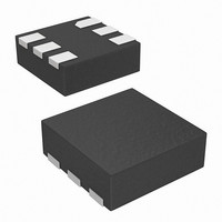
Package Outline Drawing L6.1.6x1.6 6 LEAD ULTRA THIN DUAL FLAT NO-LEAD COL PLASTIC PACKAGE (UTDFN COL) Rev 1, 11/07 1.60 6 PIN 1 INDEX AREA (4X) 0.15 TOP VIEW ( ...