ISL65426IRZA Intersil, ISL65426IRZA Datasheet - Page 14
ISL65426IRZA
Manufacturer Part Number
ISL65426IRZA
Description
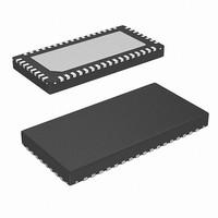
IC REG DUAL SYNC BUCK 6A 50-QFN
Manufacturer
Intersil
Type
Step-Down (Buck)r
Datasheet
1.ISL65426HRZ.pdf
(22 pages)
Specifications of ISL65426IRZA
Internal Switch(s)
Yes
Synchronous Rectifier
Yes
Number Of Outputs
2
Voltage - Output
1 ~ 4 V
Current - Output
6A
Frequency - Switching
1MHz
Voltage - Input
3 ~ 5.5 V
Operating Temperature
-40°C ~ 85°C
Mounting Type
Surface Mount
Package / Case
50-VQFN
Package
50QFN EP
Minimum Input Voltage
3 V
Maximum Input Voltage
5.5 V
Switching Frequency
1000 KHz
Operating Supply Voltage
3 to 5.5 V
Maximum Output Current
6 A
Output Type
Adjustable
Output Voltage
1 to 4 V
Efficiency
95(Typ) %
Rohs Compliant
YES
Lead Free Status / RoHS Status
Lead free / RoHS Compliant
Power - Output
-
Available stocks
Company
Part Number
Manufacturer
Quantity
Price
Company:

Part Number:
ISL65426IRZA
Manufacturer:
Intersil
Quantity:
500


Typical Performance Curves
PGND
PGND
PGND
PGND
PVIN1
PVIN2
PGND
PGND
PVIN3
PGND
VCC
VCC
VCC
LX1
LX1
LX2
LX3
10
11
12
13
14
15
16
17
8
9
1
2
3
4
5
6
7
18 19 20 21 22 23 24 25
50 49 48 47 46 45 44
PGND
14
FIGURE 34. V
43
42
41
40
39
38
37
36
35
34
33
32
31
30
29
28
27
26
Circuit of Figure 2. V
noted. Typical values are at T
V
PGND
PGND
PGND
PGND
LX6
LX6
PVIN6
PVIN5
LX5
PGND
PGND
LX4
PVIN4
PGND
PGND
GND
GND
OUT2
OUT2
LX2 5V/DIV
1V/DIV
= 3.3V OUTPUT OVERCURRENT RECOVERY
ISL65426
PG2 5V/DIV
IN
= 5V, I
Pin Descriptions
VCC
The bias supply input for the small signal circuitry. Connect
this pin to the highest supply voltage available if two or more
options are available. Locally filter this pin using a low ESL
ceramic capacitor of 1µF or larger, and a 10Ω resistor.
PVIN1, PVIN2, PVIN3, PVIN4, PVIN5, PVIN6
These pins are the power supply pins for the corresponding
PWM power blocks. Associated power blocks must all tie to
the same power supply. The power supply must fall in the
range of 3V to 5.5V.
GND
Signal ground. All small signal components connect to this
ground, which in turn connects to PGND at one point.
PGND
Power ground for the PWM power blocks and thermal relief
for the package. The exposed pad must be connected to
PGND and soldered to the PCB. Connect these pins closely
to the negative terminal of input and output capacitors.
FB1, FB2
Voltage feedback input. Depending on the voltage selection
pin settings, connect an optional resistor divider between
V
LX1, LX2, LX3, LX4, LX5, LX6
Switch node connection to inductor. This pin connects to the
internal synchronous power MOSFET switches. The
average voltage of this node is equal to the regulator output
voltage.
OUT
A
OUT1
= +25°C. (Continued)
and GND for selection of a variable output voltage.
= 4A, I
IL2 5A/DIV
OUT2
= 2A, T
A
= -10°C to +100°C unless otherwise
March 25, 2008
FN6340.3
Related parts for ISL65426IRZA
Image
Part Number
Description
Manufacturer
Datasheet
Request
R

Part Number:
Description:
6A Dual Synchronous Buck Regulator
Manufacturer:
Intersil Corporation

Part Number:
Description:
ISL65426 EVAL BOARD 1 - RoHS COMPLIANT - QFN
Manufacturer:
Intersil
Datasheet:
Part Number:
Description:
Intersil Corporation [CMOS Serial Controller Interface]
Manufacturer:
Intersil Corporation
Datasheet:
Part Number:
Description:
Manufacturer:
Intersil Corporation
Datasheet:
Part Number:
Description:
357-036-542-201 CARDEDGE 36POS DL .156 BLK LOPRO
Manufacturer:
Intersil Corporation
Datasheet:
Part Number:
Description:
1024-Word x 4-Bit LSI Static RAM
Manufacturer:
Intersil Corporation
Datasheet:
Part Number:
Description:
General Purpose NPN Transistor Arrays FN341.4
Manufacturer:
Intersil Corporation
Datasheet:
Part Number:
Description:
CMOS 16-Bit Microprocessor
Manufacturer:
Intersil Corporation
Datasheet:
Part Number:
Description:
Manufacturer:
Intersil Corporation
Datasheet:
Part Number:
Description:
Manufacturer:
Intersil Corporation
Datasheet:
Part Number:
Description:
Manufacturer:
Intersil Corporation
Datasheet:
Part Number:
Description:
Manufacturer:
Intersil Corporation
Datasheet:
Part Number:
Description:
CMOS 6-Bit Latch and Decoder Memory Interfaces
Manufacturer:
Intersil Corporation
Datasheet:
Part Number:
Description:
CA3046General Purpose NPN Transistor Arrays
Manufacturer:
Intersil Corporation
Datasheet:
Part Number:
Description:
Manufacturer:
Intersil Corporation
Datasheet: