ISL65426IRZA Intersil, ISL65426IRZA Datasheet - Page 15
ISL65426IRZA
Manufacturer Part Number
ISL65426IRZA
Description
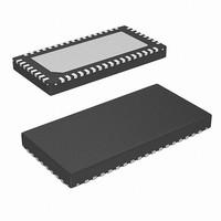
IC REG DUAL SYNC BUCK 6A 50-QFN
Manufacturer
Intersil
Type
Step-Down (Buck)r
Datasheet
1.ISL65426HRZ.pdf
(22 pages)
Specifications of ISL65426IRZA
Internal Switch(s)
Yes
Synchronous Rectifier
Yes
Number Of Outputs
2
Voltage - Output
1 ~ 4 V
Current - Output
6A
Frequency - Switching
1MHz
Voltage - Input
3 ~ 5.5 V
Operating Temperature
-40°C ~ 85°C
Mounting Type
Surface Mount
Package / Case
50-VQFN
Package
50QFN EP
Minimum Input Voltage
3 V
Maximum Input Voltage
5.5 V
Switching Frequency
1000 KHz
Operating Supply Voltage
3 to 5.5 V
Maximum Output Current
6 A
Output Type
Adjustable
Output Voltage
1 to 4 V
Efficiency
95(Typ) %
Rohs Compliant
YES
Lead Free Status / RoHS Status
Lead free / RoHS Compliant
Power - Output
-
Available stocks
Company
Part Number
Manufacturer
Quantity
Price
Company:

Part Number:
ISL65426IRZA
Manufacturer:
Intersil
Quantity:
500


EN
System enable for voltage monitoring with programmable
hysteresis. This pin has a POR rising threshold of 0.6V. This
enable is intended for applications where two or more input
power supplies are used and bias rise time is an issue.
EN1, EN2
These pins are threshold-sensitive enable inputs for the
individual PWM converters. These pins have low current
(10µA) internal pull-ups to VCC. This pin disables the
respective converter until pulled above a 1V rising threshold.
ISET1, ISET2
Power block configuration inputs. Select the proper state for
each pin according to Table 1.
V1SET1, V1SET2, V2SET1, V2SET2
Output voltage configuration inputs. Select the proper state
of each pin per the “Electrical Specifications” table.
PG1, PG2
Power-good output. Open drain logic output that is pulled to
ground when the output voltage is outside regulation limits.
Functional Description
The ISL65426 is a monolithic, constant frequency, current-
mode dual output buck converter controller with user
configurable power blocks. Designed to provide a total
DC/DC solution for FPGAs, CPLDs, core processors, and
ASICs.
Power Blocks
A unique power block architecture allows partitioning of six
1A capable modules to support one of four power block
configuration options. The block diagram in Figure 3
provides a top level view of the power block layout. One
master power block is assigned to each converter output
channel. Power Block 2 is allotted to converter Channel 1
and Power Block 5 to Channel 2. The master power blocks
must not be tied together or the controller will not soft-start.
PVIN1
PVIN2
PVIN3
LX1
LX2
LX3
FIGURE 35. POWER BLOCK DIAGRAM
POWER BLOCK 1
POWER BLOCK 2
POWER BLOCK 3
MASTER POWER BLOCK
FLOATING POWER BLOCK
15
POWER BLOCK 6
POWER BLOCK 5
POWER BLOCK 4
PVIN6
LX6
PVIN5
LX5
PVIN4
LX4
ISL65426
The remaining four floating power blocks can be partitioned
in one of four valid states outlined in Table 1. The controller
detects the programmed configuration based on the state of
logic signals at pins ISET1 and ISET2. The controller checks
the power block configuration versus the programmed
configuration before the either converter can soft-start.
Each power block has a separate power supply connection
pin, PVINx, and common channels must join these inputs to
one input power supply. Common synchronous power switch
connection points for each channel must be tied together
and to an external inductor. See the “Typical Application
Schematics” for pin connection guidance.
Each power block has a scaled pilot device providing current
feedback. The configuration pin settling determines how the
controller handles separation and summing of the individual
current feedback signals.
Main Control Loop
The ISL65426 is a monolithic, constant frequency,
current mode step-down DC/DC converter. During normal
operation, the internal top power switch is turned on at the
beginning of each clock cycle. Current in the output inductor
ramps up until the current comparator trips and turns off the
top power MOSFET. The bottom power MOSFET turns on
and the inductor current ramps down for the rest of the cycle.
The current comparator compares the output current at the
ripple current peak to a current pilot. The error amplifier
monitors V
reference. The error amplifier’s output voltage drives a
proportional current to the pilot. If V
current level is increased and the trip off current level of the
output is increased. The increased current works to raise the
V
Output Voltage Programming
The feedback voltage applied to the inverting input of the
error amplifier is scaled internally relative to the 0.6V internal
reference voltage based on the state of logic signals at pins
V1SET1, V1SET2, V2SET1 and V2SET2. The output
voltage configuration logic decodes the 2-bit voltage
identification codes into one of the discrete voltages shown
ISET1 ISET2 I
OUT
X
1
1
0
0
level into agreement with the voltage reference.
X
TABLE 1. POWER BLOCK CONFIGURATION
1
0
1
0
OUT
Invalid LX Configurations: SS Prevented
OUT1
3A
4A
5A
2A
1A
and compares it with the internal voltage
LX1,LX2,LX3,LX4
CONNECTIONS I
LX1,LX2,LX3,
LX1,LX2,LX3
CHANNEL 1
LX4,LX6
LX1,LX2
LX2
OUT
OUT2
3A
2A
1A
4A
5A
is low the pilot’s
LX3,LX4,LX5,LX6
CONNECTIONS
LX1,LX3,LX4,
LX4,LX5,LX6
CHANNEL 2
LX5,LX6
LX5,LX6
March 25, 2008
LX5
FN6340.3
Related parts for ISL65426IRZA
Image
Part Number
Description
Manufacturer
Datasheet
Request
R

Part Number:
Description:
6A Dual Synchronous Buck Regulator
Manufacturer:
Intersil Corporation

Part Number:
Description:
ISL65426 EVAL BOARD 1 - RoHS COMPLIANT - QFN
Manufacturer:
Intersil
Datasheet:
Part Number:
Description:
Intersil Corporation [CMOS Serial Controller Interface]
Manufacturer:
Intersil Corporation
Datasheet:
Part Number:
Description:
Manufacturer:
Intersil Corporation
Datasheet:
Part Number:
Description:
357-036-542-201 CARDEDGE 36POS DL .156 BLK LOPRO
Manufacturer:
Intersil Corporation
Datasheet:
Part Number:
Description:
1024-Word x 4-Bit LSI Static RAM
Manufacturer:
Intersil Corporation
Datasheet:
Part Number:
Description:
General Purpose NPN Transistor Arrays FN341.4
Manufacturer:
Intersil Corporation
Datasheet:
Part Number:
Description:
CMOS 16-Bit Microprocessor
Manufacturer:
Intersil Corporation
Datasheet:
Part Number:
Description:
Manufacturer:
Intersil Corporation
Datasheet:
Part Number:
Description:
Manufacturer:
Intersil Corporation
Datasheet:
Part Number:
Description:
Manufacturer:
Intersil Corporation
Datasheet:
Part Number:
Description:
Manufacturer:
Intersil Corporation
Datasheet:
Part Number:
Description:
CMOS 6-Bit Latch and Decoder Memory Interfaces
Manufacturer:
Intersil Corporation
Datasheet:
Part Number:
Description:
CA3046General Purpose NPN Transistor Arrays
Manufacturer:
Intersil Corporation
Datasheet:
Part Number:
Description:
Manufacturer:
Intersil Corporation
Datasheet: