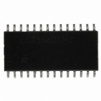
EL7556DCMZ Intersil, EL7556DCMZ Datasheet - Page 8

EL7556DCMZ
Manufacturer Part Number
EL7556DCMZ
Description
IC REG 6A DC/DC SW SD 28SOIC
Manufacturer
Intersil
Type
Step-Down (Buck)r
Datasheet
1.EL7556DCMZ.pdf
(11 pages)
Specifications of EL7556DCMZ
Internal Switch(s)
Yes
Synchronous Rectifier
Yes
Number Of Outputs
1
Voltage - Output
1 ~ 3.8 V
Current - Output
6A
Frequency - Switching
1MHz
Voltage - Input
5V
Operating Temperature
-40°C ~ 85°C
Mounting Type
Surface Mount
Package / Case
28-SOIC (7.5mm Width)
Power - Output
21W
Lead Free Status / RoHS Status
Lead free / RoHS Compliant
Available stocks
Company
Part Number
Manufacturer
Quantity
Price
Pin Descriptions
I = Input, O = Output, S = Supply
NUMBER
PIN
10
11
12
13
14
15
16
17
18
19
20
21
22
23
24
25
26
27
28
1
2
3
4
5
6
7
8
9
PIN NAME
VCC2DET
CSLOPE
PWRGD
OUTEN
COSC
CREF
VSSP
VSSP
VSSP
VSSP
VSSP
VSSP
VSSP
TEST
VDD
VSS
FB1
C2V
FB2
VIN
VIN
VHI
OT
CP
LX
LX
LX
LX
PIN TYPE
8
O
S
S
S
S
S
S
S
S
O
S
S
O
O
O
O
S
O
I
I
I
I
I
I
I
I
I
I
Voltage feedback pin for the buck regulator. Active when VCC2DET is logic low. Normally connected to
external resistor divider between V
that FB1 is floating and VCC2DET is inadvertently connected to GND.
Bandgap reference bypass capacitor. Typically 0.1µF to V
Slope compensation capacitor. Ramp width corresponds to LX duty cycle. C
normally 1:1.5.
Oscillator timing capacitor. F
Farads.
Power Supply for PWM control circuitry. Normally the same potential as V
Power supply for the buck regulator. Connected to the drain of the high-side NMOS FET.
Ground return for the buck regulator. Connected to the source of the low-side synchronous NMOS FET.
Same as pin 6.
Same as pin 7.
Same as pin 7.
Same as pin 7.
Same as pin 7.
VCC2DET interface logic input. When driven to logic 1 V
uses FB1 to determine V
The switching regulator output is enabled when logic 1. The reference voltage output operates whenever
the power supply is qualified (V
Over temperature indicator. Normally high. Pulls low when die temperature exceeds 135°C, returns to
the high state when die temperature has cooled to 100°C.
Power good window comparator output. Logic 1 when regulator output is within ±10% of programmed
voltage.
Test pin. Must be connected to VSSP in normal operation.
Same as pin 7.
Same as pin 7.
Inductor drive pin. High current switching output whose average voltage equals the regulator output
voltage.
Same as pin 20.
Same as pin 20.
Same as pin 20.
Gate drive to high-side driver. Bootstrapped from LX with a 0.1µF capacitor.
Ground return for the control circuitry.
Connected to voltage doubler output. Supplies gate drive to the low-side driver.
Drives the negative side of charge pump capacitor at one-half the oscillator frequency F
Voltage feedback pin. Active when VCC2DET is logic 1. Internally preset to V
EL7556D
OUT
OSC
: V
DD
OUT
(Hz) can be approximated by: F
OUT
>VPOR) regardless of the state of this pin.
= 1.0V*(1+R3/R4).
and GND. A 2µA pull-up current forces V
FUNCTION
OUT
SS
= 3.500V. When driven to logic 0 the PWM
.
OSC
(Hz) = 0.0001/C
IN
.
SLOPE
OUT
OUT
= 3.5V.
to C
to V
OSC
SS
OSC
OSC
. C
in the event
.
OSC
ratio is
in


