HW-USB-II-G Xilinx Inc, HW-USB-II-G Datasheet - Page 19
HW-USB-II-G
Manufacturer Part Number
HW-USB-II-G
Description
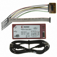
PLATFORM CABLE USB II
Manufacturer
Xilinx Inc
Datasheet
1.HW-USB-II-G.pdf
(35 pages)
Specifications of HW-USB-II-G
Accessory Type
USB Platform Cable
For Use With/related Products
Xilinx FPGA, CPLDS, Platform Flash PROMs, XC18V00 PROMs, System ACE MPM
Lead Free Status / RoHS Status
Lead free / RoHS Compliant
Other names
122-1572
Available stocks
Company
Part Number
Manufacturer
Quantity
Price
Company:

Part Number:
HW-USB-II-G
Manufacturer:
APEC
Quantity:
4 000


For a complete description on using Platform Cable USB II for indirect programming of third-BPI PROMs and for a complete
list of supported BPI PROMs, refer to XAPP973, Indirect Programming of BPI PROMs with Virtex-5 FPGAs.
Target Interface Reference Voltage and Signals
Target Reference Voltage Sensing (VREF)
Platform Cable USB II incorporates an over-voltage clamp on the V
clamped voltage (V
Structure). V
Note:
When Platform Cable USB II is idle, a nominal amount of current is drawn from the target system V
V
No damage to Platform Cable USB II occurs if the A–B cable is unplugged from the host while the ribbon cable or flying leads
are attached to a powered target system. Similarly, no damage to target systems occurs if Platform Cable USB II is powered
and attached to the target system while the target system power is off.
Bidirectional Signal Pins
Platform Cable USB II provides five bidirectional signal pins: TDI_DIN_MOSI, TDO_DONE_MISO, TCK_CCLK_SCK,
TMS_PROG_SS and HALT_INT_WP. Each pin incorporates the same I/O structure. The state of each pin (reading or
writing) is determined by the current mode of the cable (JTAG, SPI or Slave Serial).
Output Driver Structure
Each output signal is routed through a NC7SZ126 ultra high-speed CMOS buffer
resistors (30.1Ω) reduce reflections. Weak pull-up resistors (20 kΩ) terminating at V
when the buffers are set to high-Z. Schottky diodes provide the output buffers with undershoot protection.
The FPGA sets the output buffers to high-Z when V
clamps V
Figure 21, page 21
Note:
Xilinx design tools actively drive the outputs to logic 1 before setting the respective buffer to high-Z, avoiding the possibility
of a slow rise-time transition caused by a charge path through the pull-up resistor into parasitic capacitance on the target
system.
DS593 (v1.2.1) March 17, 2011
REF
current as a function of V
Do not insert a current-limiting resistor in the target system between the V
The output drivers are enabled only during cable operations; otherwise, they are set to high-Z between operations.
REF_CLAMP
REF
must be a regulated voltage.
REF_CLAMP
shows the relationship between the output drive voltage and V
to approximately 3.9V.
) supplies high-slew-rate buffers that drive each of the output signals (see
REF
voltage.
REF
www.xilinx.com
drops below 1.30 V. In addition, an over-voltage Zener on V
REF
pin of the 2-mm ribbon cable connector. The
REF
supply and pin 2 on the 2-mm connector.
(Figure 20, page
REF_CLAMP
REF
.
maintain a defined logic level
REF
20). Series-damping
Platform Cable USB II
.
Figure 19
Output Driver
shows the
REF
19
Related parts for HW-USB-II-G
Image
Part Number
Description
Manufacturer
Datasheet
Request
R

Part Number:
Description:
PLATFORM CABLE USB
Manufacturer:
Xilinx Inc
Datasheet:

Part Number:
Description:
IC CABLE
Manufacturer:
Xilinx Inc
Datasheet:

Part Number:
Description:
BOARD ADAPTER AND FLY LEADS
Manufacturer:
Xilinx Inc
Datasheet:

Part Number:
Description:
XLXHW-LICENSE-DONGLE-USB-G USB DONGLE OP
Manufacturer:
Xilinx Inc

Part Number:
Description:
IC CPLD .8K 36MCELL 44-VQFP
Manufacturer:
Xilinx Inc
Datasheet:

Part Number:
Description:
IC CPLD 72MCRCELL 10NS 44VQFP
Manufacturer:
Xilinx Inc
Datasheet:

Part Number:
Description:
IC CPLD 1.6K 72MCELL 64-VQFP
Manufacturer:
Xilinx Inc
Datasheet:

Part Number:
Description:
IC CR-II CPLD 64MCELL 44-VQFP
Manufacturer:
Xilinx Inc
Datasheet:

Part Number:
Description:
IC CPLD 1.6K 72MCELL 100-TQFP
Manufacturer:
Xilinx Inc
Datasheet:

Part Number:
Description:
IC CR-II CPLD 64MCELL 56-BGA
Manufacturer:
Xilinx Inc
Datasheet:

Part Number:
Description:
IC CPLD 72MCRCELL 7.5NS 44VQFP
Manufacturer:
Xilinx Inc
Datasheet:
Part Number:
Description:
IC CR-II CPLD 64MCELL 100-VQFP
Manufacturer:
Xilinx Inc
Datasheet:
Part Number:
Description:
IC CPLD 1.6K 72MCELL 100-TQFP
Manufacturer:
Xilinx Inc
Datasheet:

Part Number:
Description:
IC CPLD 72MCRCELL 7.5NS 64VQFP
Manufacturer:
Xilinx Inc
Datasheet:
Part Number:
Description:
IC CPLD 1.6K 72MCELL 100-TQFP
Manufacturer:
Xilinx Inc
Datasheet: