HW-USB-II-G Xilinx Inc, HW-USB-II-G Datasheet - Page 22
HW-USB-II-G
Manufacturer Part Number
HW-USB-II-G
Description
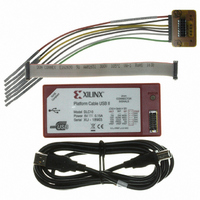
PLATFORM CABLE USB II
Manufacturer
Xilinx Inc
Datasheet
1.HW-USB-II-G.pdf
(35 pages)
Specifications of HW-USB-II-G
Accessory Type
USB Platform Cable
For Use With/related Products
Xilinx FPGA, CPLDS, Platform Flash PROMs, XC18V00 PROMs, System ACE MPM
Lead Free Status / RoHS Status
Lead free / RoHS Compliant
Other names
122-1572
Available stocks
Company
Part Number
Manufacturer
Quantity
Price
Company:

Part Number:
HW-USB-II-G
Manufacturer:
APEC
Quantity:
4 000


Pseudo Ground Signal
The pseudo ground (PGND) pin on target interface connector is routed to a ultra-high-speed buffer with an open-drain output
(Figure
as high as 6.0V.
X-Ref Target - Figure 23
HALT_INIT_WP Signal in iMPACT
Platform Cable USB II provides a second multi-use signal on its target interface connector called HALT_INIT_WP (this signal
is referred to as HALT when the cable is in JTAG mode). The HALT_INIT_WP pin is connected to a three-state CMOS driver
(see
The behavior of HALT_INIT_WP is determined by the host application connected to the cable. iMPACT provides the option
of enabling the HALT pin during JTAG operations
iMPACT GUI and selecting Edit → Set Programming Properties… to open the Device Programming Properties dialog box.
Check “Assert Cable INIT during programming” to enable the HALT signal.
When enabled in iMPACT, HALT is active-Low while the cable is performing JTAG operations on any Xilinx FPGA and high-
Z when the cable is idle. HALT is active-High while JTAG operations are being performed on other devices. The HALT signal
remains high-Z when not enabled (iMPACT default) or when the cable is in Slave Serial or SPI modes.
Note:
tools where the HALT signal is not supported.
DS593 (v1.2.1) March 17, 2011
Bidirectional Signal Pins, page
HALT signal control is available in iMPACT 9.2i and later. HALT remains high-Z in earlier versions of iMPACT and in Xilinx design
23). A pull-up resistor is required on target systems that utilize this signal. The buffer can tolerate a pull-up voltage
FPGA
19).
PGND_CNTL
Figure 23: PGND Signal
(Figure
NC7WZ07
www.xilinx.com
24). This option is accessed by clicking on the Xilinx FPGA in the
A
Y
2-mm Connector
Input
PGND
H
A
L
DS593_23_021508
Output
Y
Z
L
Platform Cable USB II
22
Related parts for HW-USB-II-G
Image
Part Number
Description
Manufacturer
Datasheet
Request
R

Part Number:
Description:
PLATFORM CABLE USB
Manufacturer:
Xilinx Inc
Datasheet:

Part Number:
Description:
IC CABLE
Manufacturer:
Xilinx Inc
Datasheet:

Part Number:
Description:
BOARD ADAPTER AND FLY LEADS
Manufacturer:
Xilinx Inc
Datasheet:

Part Number:
Description:
XLXHW-LICENSE-DONGLE-USB-G USB DONGLE OP
Manufacturer:
Xilinx Inc

Part Number:
Description:
IC CPLD .8K 36MCELL 44-VQFP
Manufacturer:
Xilinx Inc
Datasheet:

Part Number:
Description:
IC CPLD 72MCRCELL 10NS 44VQFP
Manufacturer:
Xilinx Inc
Datasheet:

Part Number:
Description:
IC CPLD 1.6K 72MCELL 64-VQFP
Manufacturer:
Xilinx Inc
Datasheet:

Part Number:
Description:
IC CR-II CPLD 64MCELL 44-VQFP
Manufacturer:
Xilinx Inc
Datasheet:

Part Number:
Description:
IC CPLD 1.6K 72MCELL 100-TQFP
Manufacturer:
Xilinx Inc
Datasheet:

Part Number:
Description:
IC CR-II CPLD 64MCELL 56-BGA
Manufacturer:
Xilinx Inc
Datasheet:

Part Number:
Description:
IC CPLD 72MCRCELL 7.5NS 44VQFP
Manufacturer:
Xilinx Inc
Datasheet:
Part Number:
Description:
IC CR-II CPLD 64MCELL 100-VQFP
Manufacturer:
Xilinx Inc
Datasheet:
Part Number:
Description:
IC CPLD 1.6K 72MCELL 100-TQFP
Manufacturer:
Xilinx Inc
Datasheet:

Part Number:
Description:
IC CPLD 72MCRCELL 7.5NS 64VQFP
Manufacturer:
Xilinx Inc
Datasheet:
Part Number:
Description:
IC CPLD 1.6K 72MCELL 100-TQFP
Manufacturer:
Xilinx Inc
Datasheet: