HW-USB-II-G Xilinx Inc, HW-USB-II-G Datasheet - Page 29
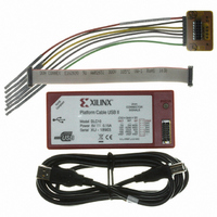
HW-USB-II-G
Manufacturer Part Number
HW-USB-II-G
Description
PLATFORM CABLE USB II
Manufacturer
Xilinx Inc
Datasheet
1.HW-USB-II-G.pdf
(35 pages)
Specifications of HW-USB-II-G
Accessory Type
USB Platform Cable
For Use With/related Products
Xilinx FPGA, CPLDS, Platform Flash PROMs, XC18V00 PROMs, System ACE MPM
Lead Free Status / RoHS Status
Lead free / RoHS Compliant
Other names
122-1572
Available stocks
Company
Part Number
Manufacturer
Quantity
Price
Company:

Part Number:
HW-USB-II-G
Manufacturer:
APEC
Quantity:
4 000


X-Ref Target - Figure 30
Interface Pin Descriptions
Table 6: JTAG/SPI/Slave Serial Port: 2-mm Connector Signals
DS593 (v1.2.1) March 17, 2011
Number
Pin
2
4
6
8
speed — degraded
full speed because
12 Mb/s Bus Speed
to slow bus speed
Platform Cable
performance due
1.X Root Hub
Enumerates at
operates at full
root hub only
USB II
Configuration
(A)
500
mA
JTAG
V
TMS
TDO
TCK
REF
Figure 30: Platform Cable USB II Performance with Various Hub Types
12 Mb/s Bus Speed
Programming
1.X Root Hub
Bus-Powered
2.0 External
MODE
speed — degraded
full speed because
Hub
V
Platform Cable
to slow bus speed
performance due
SPI
(B)
Enumerates at
operates at full
REF
–
–
–
root hub only
500
mA
USB II
(1)
< 500
mA
Power
Configuration
Slave-Serial
480 Mb/s Bus Speed
Self-Powered
2.0 Root Hub
V
2.0 External
REF
www.xilinx.com
–
–
–
Enumerates at full speed
performance due to slow
bus speed. Cable may
because 2.0 external
hub operates at full
speed — degraded
Hub
Platform Cable
(C)
not enumerate.
500
mA
USB II
< 500
mA
Direction
Power
Out
Out
In
In
480 Mb/s Bus Speed
Self-Powered
2.0 Root Hub
2.0 External
(2)
Hub
performance due to
Platform Cable
(D)
Hi-Speed — best
high bus speed.
Enumerates at
Target Reference Voltage
should be connected to a voltage bus on the
target system that serves the JTAG, SPI or
Slave Serial interface. For example, when
programming a CoolRunner-II device using
JTAG, V
target V
JTAG Test Mode Select. This pin is the
JTAG mode signal establishing appropriate
TAP state transitions for target ISP devices
sharing the same data stream.
JTAG Test Clock. This pin is the clock
signal for JTAG operations and should be
connected to the TCK pin on all target ISP
devices sharing the same data stream.
JTAG Test Data Out. This pin is the serial
data stream received from the TDO pin on
the last device in a JTAG chain.
500
mA
USB II
500
mA
AUX
REF
bus.
should be connected to the
480 Mb/s Bus Speed
Platform Cable
Description
performance due to
2.0 Root Hub
Hi-Speed — best
high bus speed.
Enumerates at
Platform Cable USB II
USB II
(E)
500
mA
(3)
DS593_30_021408
. This pin
29
Related parts for HW-USB-II-G
Image
Part Number
Description
Manufacturer
Datasheet
Request
R

Part Number:
Description:
PLATFORM CABLE USB
Manufacturer:
Xilinx Inc
Datasheet:

Part Number:
Description:
IC CABLE
Manufacturer:
Xilinx Inc
Datasheet:

Part Number:
Description:
BOARD ADAPTER AND FLY LEADS
Manufacturer:
Xilinx Inc
Datasheet:

Part Number:
Description:
XLXHW-LICENSE-DONGLE-USB-G USB DONGLE OP
Manufacturer:
Xilinx Inc

Part Number:
Description:
IC CPLD .8K 36MCELL 44-VQFP
Manufacturer:
Xilinx Inc
Datasheet:

Part Number:
Description:
IC CPLD 72MCRCELL 10NS 44VQFP
Manufacturer:
Xilinx Inc
Datasheet:

Part Number:
Description:
IC CPLD 1.6K 72MCELL 64-VQFP
Manufacturer:
Xilinx Inc
Datasheet:

Part Number:
Description:
IC CR-II CPLD 64MCELL 44-VQFP
Manufacturer:
Xilinx Inc
Datasheet:

Part Number:
Description:
IC CPLD 1.6K 72MCELL 100-TQFP
Manufacturer:
Xilinx Inc
Datasheet:

Part Number:
Description:
IC CR-II CPLD 64MCELL 56-BGA
Manufacturer:
Xilinx Inc
Datasheet:

Part Number:
Description:
IC CPLD 72MCRCELL 7.5NS 44VQFP
Manufacturer:
Xilinx Inc
Datasheet:
Part Number:
Description:
IC CR-II CPLD 64MCELL 100-VQFP
Manufacturer:
Xilinx Inc
Datasheet:
Part Number:
Description:
IC CPLD 1.6K 72MCELL 100-TQFP
Manufacturer:
Xilinx Inc
Datasheet:

Part Number:
Description:
IC CPLD 72MCRCELL 7.5NS 64VQFP
Manufacturer:
Xilinx Inc
Datasheet:
Part Number:
Description:
IC CPLD 1.6K 72MCELL 100-TQFP
Manufacturer:
Xilinx Inc
Datasheet: