ATA6823-DK Atmel, ATA6823-DK Datasheet - Page 7
ATA6823-DK
Manufacturer Part Number
ATA6823-DK
Description
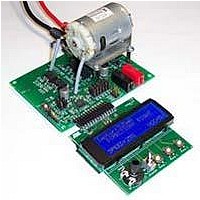
BOARD EVALUATION FOR ATA6823
Manufacturer
Atmel
Type
PWM Controllersr
Specifications of ATA6823-DK
Main Purpose
Power Management, Motor Control
Embedded
No
Utilized Ic / Part
ATA6823
Primary Attributes
Brush DC Motors, 8 ~ 18V, LIN Interface, Watchdog, 5V Regulator
Secondary Attributes
Cross Conduction, Under/Over Voltage, Short Circuit, & Temperature Protection
Input Voltage
8 V to 18 V
Product
Power Management Modules
Lead Free Status / RoHS Status
Contains lead / RoHS non-compliant
For Use With/related Products
ATA6823


3.4
4856K–AUTO–01/11
5V/3.3V VCC Regulator
Figure 3-1
vated receive block of the LIN interface. After going to Active mode, the V
working.
Go to Sleep is possible with a valid HIGH to LOW transition at pin EN1 (permanent LOW for
longer than t
Switching characteristic of the outputs:
When the IC is set to SLEEP MODE by a “high to low” transition at pin EN1, the low-side tran-
sistors of the external H-bridge are switched on for a short time. This causes a shortcircuit
current pulse in the bridge because one of the high-side transistors is usually on. The pulse
length is similar to the one of the implemented short circuit detection time t
of the external FETs it needs to be considered that in the case of a short circuit condition the
current in the transistors will flow for a time t
“Electrical Characteristics” on page
short circuit behavior has to be taken into consideration, so that they will not be damaged in
the event of a short circuit condition caused by a failure or caused by the described sleep
mode switching.
Figure 3-1.
The 5V/3.3V regulator is fully integrated on-chip. It requires only a 2.2µF ceramic capacitor for
stability and has 100 mA current capability. Using the VMODE pin, the output voltage can be
selected to either 5V or 3.3V. Switching of the output voltage during operation is not intended
to be supported. The VMODE pin must be hard-wired to either VINT for 5V or to GND for 3.3V.
The logic HIGH level of the microcontroller interface will be adapted to the VCC regulator
voltage.
The output voltage accuracy is in general < ±3%; in the 5V mode with V
< 5%.
To prevent destruction of the IC, the current delivered by the regulator is limited to maximum
100mA to 350mA. The delivered voltage will break down and a reset may occur.
illustrates the wake-up by LIN. The status PREWAKE is characterized by the acti-
VCC
EN1
LIN
db
) if EN1 was in a valid HIGH state (HIGH for longer than t
Wake-up by pin LIN
Active Mode
T
gotosleep
= 20 µs
17, item 7.29. For the selection of the external FETs this
Sleep Mode
sc
T w
with a maximum of 15µs according to
akelin
= 70 µs
Regulator Wake-up Time
Atmel ATA6823
Active Mode
VBAT
db
) before.
sc
CC
< 9V it is limited to
. For the selection
regulator starts
Section 8.
7
Related parts for ATA6823-DK
Image
Part Number
Description
Manufacturer
Datasheet
Request
R

Part Number:
Description:
IC H-BRIDGE MOTOR DRIVER 32-QFN
Manufacturer:
Atmel
Datasheet:

Part Number:
Description:
Motor / Motion / Ignition Controllers & Drivers Gate Driver IC
Manufacturer:
Atmel
Datasheet:

Part Number:
Description:
H-bridge Motor Driver
Manufacturer:
ATMEL Corporation
Datasheet:

Part Number:
Description:
DEV KIT FOR AVR/AVR32
Manufacturer:
Atmel
Datasheet:
Part Number:
Description:
INTERVAL AND WIPE/WASH WIPER CONTROL IC WITH DELAY
Manufacturer:
ATMEL Corporation
Datasheet:
Part Number:
Description:
Low-Voltage Voice-Switched IC for Hands-Free Operation
Manufacturer:
ATMEL Corporation
Datasheet:
Part Number:
Description:
MONOLITHIC INTEGRATED FEATUREPHONE CIRCUIT
Manufacturer:
ATMEL Corporation
Datasheet:
Part Number:
Description:
AM-FM Receiver IC U4255BM-M
Manufacturer:
ATMEL Corporation
Datasheet:
Part Number:
Description:
Monolithic Integrated Feature Phone Circuit
Manufacturer:
ATMEL Corporation
Datasheet:
Part Number:
Description:
Multistandard Video-IF and Quasi Parallel Sound Processing
Manufacturer:
ATMEL Corporation
Datasheet:
Part Number:
Description:
High-performance EE PLD
Manufacturer:
ATMEL Corporation
Datasheet:
Part Number:
Description:
8-bit Flash Microcontroller
Manufacturer:
ATMEL Corporation
Datasheet: