EVAL6569 STMicroelectronics, EVAL6569 Datasheet - Page 4
EVAL6569
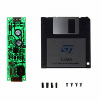
Manufacturer Part Number
EVAL6569
Description
BOARD EVAL LIGHTING L6569
Manufacturer
STMicroelectronics
Type
Charge Pumpsr
Datasheet
1.EVAL6569.pdf
(14 pages)
Specifications of EVAL6569
Mfg Application Notes
L6569, AN880 App Note
Main Purpose
Lighting, Ballast Control
Embedded
No
Utilized Ic / Part
L6569
Primary Attributes
18 W, Optimized for a CF18DT/E/830, 120 or 230 VAC
Secondary Attributes
Preheating Done with a PTC
Input Voltage
230 V
Product
Power Management Modules
Supply Current
0.17 A
Lead Free Status / RoHS Status
Lead free / RoHS Compliant
For Use With/related Products
L6569
Other names
497-4738


AN880 APPLICATION NOTE
The L6569A holds both MOSFETs OFF until the
Under Voltage Lock Out is reached. This is in-
tended for inverters using 2 decoupling capacitors
in half bridge as shown on figure 12. The inverter
is totally off, so that the voltage at the capacitors
center node is not unbalanced by the leakage
path during power on.
CONSIDERATIONS ON THE L6569 ENVIRON-
MENT
To illustrate the benefits of the L6569 in the CFL
applications, a demonstration board was devel-
oped to supply Sylvania 18W DULUX lamp (ref:
CF18DT/E). The following chapters summarize
the application considerations applied in this de-
sign. The schematic, lay out and components list
are shown in appendix A.
Symmetric half bridge operation
To supply a fluorescent lamp, the ballast has to
achieve 3 functions: pre heat, ignition, and normal
lamp operation. The serial resonance occurs be-
tween the choke and the capacitor in parallel with
the lamp. The choice of these components deter-
mines the lamp ignition voltage and the nominal
lamp current.
Since the inverter using the L6569 and MOSFETs
can operate at a higher frequency than conven-
tional solutions, the size of the passive compo-
nents will be reduced. Such inverter can operate
up to 150 kHz in ZVS mode, and the switching
losses of the power transistors only limits the fre-
quency. In new design this frequency should be
set between 50 and 100 kHz. For instance with
an 18W lamp, a frequency increase from 33 to 50
kHz will lead to a 40% reduction of the choke
size.
To operate in Zero Voltage Switching (ZVS), the
switching frequency is higher than the resonant
frequency. All operation phases of the ballast are
secure in this mode. When the bootstrap transis-
tor is conducting, no pulse current will flow from
pin BOOT to pin V
Current Switching. The bootstrap transistor re-
mains in its Safe Operating Area, and its dissipa-
tion is negligible.
The MOSFET drive
The ZVS drive technique requires only a fast turn
off capability as shown on figure 2, and the tran-
sistor buffers are designed with a stronger sink
current. The two MOSFET buffers of the L6569
can sink a 400 mA peak current on capacitive
load. Typically these buffers can drive any MOS-
FETs in TO220 package.
Figure 7 shows an example with the STP8NA50
that has an 0.85
4/14
resistance R
S
, as it might happen in Zero
DS-ON
.
Figure 7: Current and voltage of the STP8NA50
The built-in dead time circuit acts when a MOS-
FET turns off, delaying the turn on of the opposite
transistor for 1.25 s. The voltage V
the 2 MOSFETs must switch within the minimum
dead time (0.85
avoid bridge cross conductions and transistors
overheat.
Figure 8: STD3NA50 MOSFET turn off when
The MOSFET voltage selection
Since the ballast is connected to the ac mains, it
must handle any spurious voltage spikes. When
the front end RFI filter and the clamping device,
such as a varistor, absorbes totally the spike en-
ergy, MOSFETs can have the same 600V mini-
mum breakdown voltage BV
Otherwise when the upper MOSFET is on, the re-
sidual default may be applied to the L6569. Al-
though the pin OUT breakdown voltage is higher
than 600V, it has a poor avalanche robustness.
Therefore the lower MOSFET protects the driver
by having a lower BV
mum BV
task.
I
V
V
D
I
GS
D
D
DSS
MOSFET at turn off with the L6569.
T
@ Tj = 50°C, RG = 22 .
driven by the L6569. T
GD
50 ns/dv ; 1 A/dv ; 5 V/dv ; 50V/dv
200 ns/dv ; 50 V/dv ; 0.1 A/dv
up to 500V will achieve safely this
= 245 ns ,Tc = 95 ns, E = 93 J
T
T
GD
C
s), as shown on figure 8, to
DSS
T
D
T
. A MOSFET with a mini-
GD
DSS
Tc
as the L6569.
C
+ T
LVG
RF
OUT
GD
V
DS
between
< T
D
GND
GND
GND
GND
GND
GND
Related parts for EVAL6569
Image
Part Number
Description
Manufacturer
Datasheet
Request
R

Part Number:
Description:
STMicroelectronics [RIPPLE-CARRY BINARY COUNTER/DIVIDERS]
Manufacturer:
STMicroelectronics
Datasheet:
Part Number:
Description:
STMicroelectronics [LIQUID-CRYSTAL DISPLAY DRIVERS]
Manufacturer:
STMicroelectronics
Datasheet:

Part Number:
Description:
BOARD EVAL FOR MEMS SENSORS
Manufacturer:
STMicroelectronics
Datasheet:
Part Number:
Description:
NPN TRANSISTOR POWER MODULE
Manufacturer:
STMicroelectronics
Datasheet:
Part Number:
Description:
TURBOSWITCH ULTRA-FAST HIGH VOLTAGE DIODE
Manufacturer:
STMicroelectronics
Datasheet:
Part Number:
Description:
Manufacturer:
STMicroelectronics
Datasheet:
Part Number:
Description:
DIODE / SCR MODULE
Manufacturer:
STMicroelectronics
Datasheet:
Part Number:
Description:
DIODE / SCR MODULE
Manufacturer:
STMicroelectronics
Datasheet:
Part Number:
Description:
Search -----> STE16N100
Manufacturer:
STMicroelectronics
Datasheet:
Part Number:
Description:
Search ---> STE53NA50
Manufacturer:
STMicroelectronics
Datasheet:
Part Number:
Description:
NPN Transistor Power Module
Manufacturer:
STMicroelectronics
Datasheet:
Part Number:
Description:
DIODE / SCR MODULE
Manufacturer:
STMicroelectronics
Datasheet: